Introduction
In recent years, carbon nanotubes, with high tensile strength and electrical conductivity, have been used in polymer composites to improve their mechanical and electrical properties. As a result, nanotube-polymer composites have been explored as a new class of materials. In particular, single-walled carbon nanotubes (SWNTs) have outstanding charge transport and are becoming more and more attractive as additives for semiconducting polymers, such as poly-3-hexylthiophene (P3HT) one of the most common ones used today, or insulating polymers, such as polystyrene (PS) [1–3].
Nanotube-polymer composites have been used to produce electrically conductive adhesives and enhanced piezoelectric polymers [1–3]. Current devices exploiting SWNTs include broadband photodetectors, hybrid and organic solar cells, electrically conductive photonic crystals, and photothermal composites for biomedical use. In many of these applications, formation of a continuous (percolated) network of interconnected nanotubes inside a polymer film is essential for increasing the film performance by preventing nanotube aggregation and promoting charge transport.
Recently, it has been shown that ultrafast charge transport readily occurs at the interface between the SWNTs and the polymer matrix [1–3]. The nanotubes act as highly efficient pathways for charge transport between the polymer composite interface and an electrode. Many methods used to form nanotube networks for electronic applications produce a random network, often difficult to reproduce, yielding inefficient charge transport [1–3]. These methods usually exploit spin-coating or drop casting from solution, but no microscale or nanoscale engineering. The formation of a continuous, percolated network of interconnected nanotubes inside a polymer matrix is important for better charge transport and reliable electrical properties. For this purpose, 3D nano-engineered arrays of SWNT nanoscale and microscale networks in a polymer matrix, such as P3HT or PS (refer to Figure 1), produce efficient charge transport even at very low nanotube concentrations (loading) and low voltages. An increase in conductivity up to 100 times is observed when compared to a random nanotube network inside a semiconducting polymer, such as P3HT, and up to 100 million times in an insulating polymer, such as PS. In addition, the SWNT-polymer composites imprinted with nanostructures achieved greater conductivity than those with microstructures.
The method described here allows the formation of well-ordered nanoscale and microscale domains of continuous, interconnected SWNT networks [1–3]. The method is compatible with large area imprinting and roll-to-roll processes of polymer composites making it easy to use with production methods for optoelectronic and photovoltaic devices. It is believed that the next generation of hybrid and organic photovoltaic devices could be made from carbon nanotubes and semiconducting polymers.
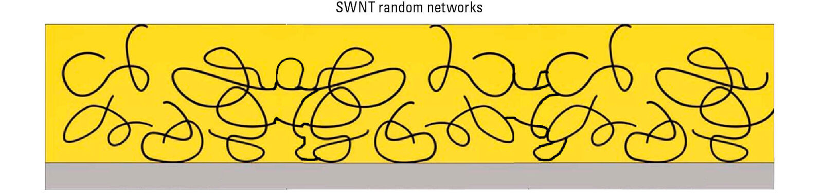
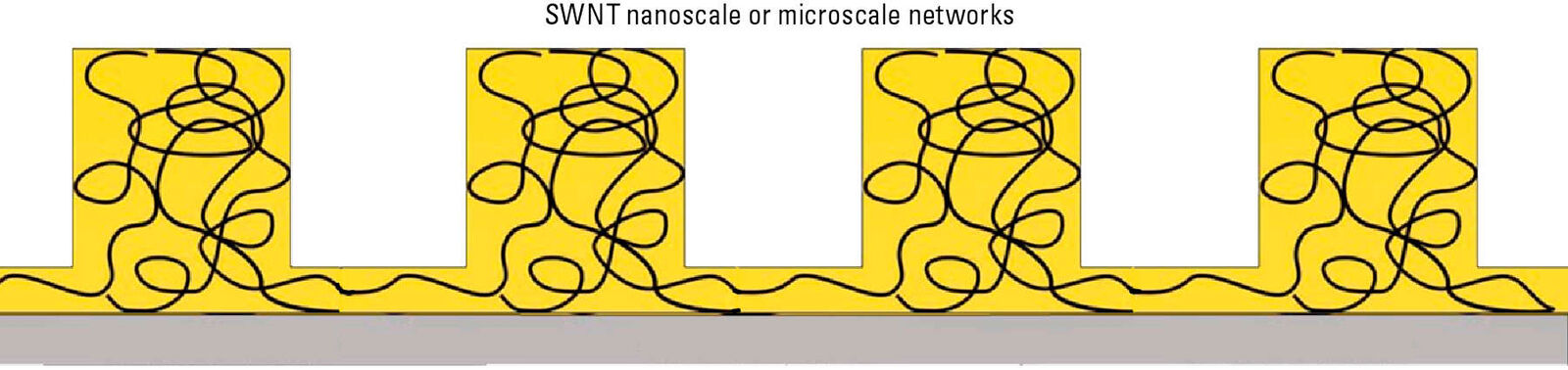
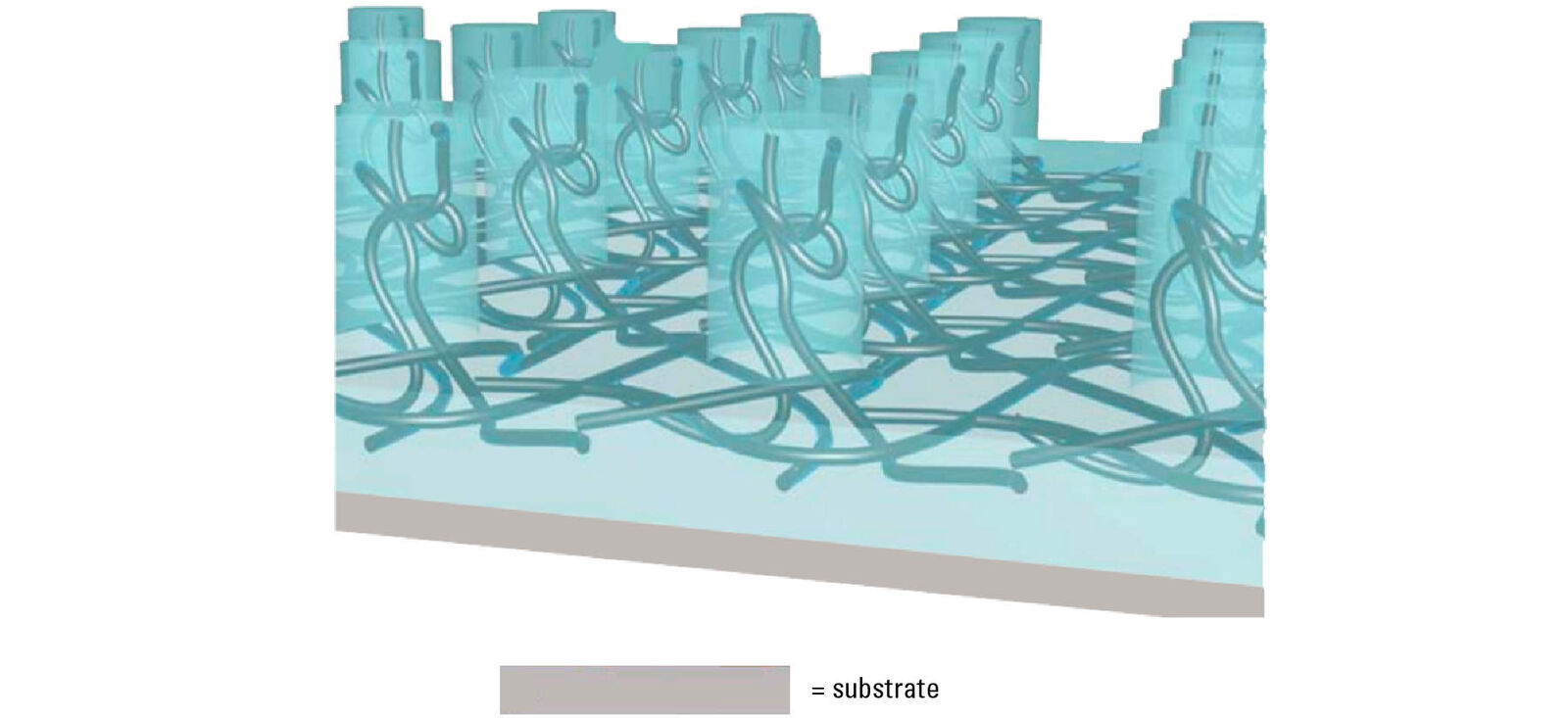
Fig. 1: SWNT-polymer composite: A) random network, B) network within imprinted nano- or micro-structures, and C) 3D view of nanotube nanoscale or microscale networks.
Methods and materials
Nano-structured and micro-structured films
The single-walled nanotubes (SWNTs) were mostly semiconducting (>90 %) and used as purchased without any purification or doping. They were dispersed and ultrasonicated in an organic solvent.
The SWNT nanoscale and microscale networks [1, 2] were produced in the following way:
- forming a thin layer of nanotubes onto a doped, conductive silicon (Si) substrate (resistivity 0.002–0.005 Ω•cm) with spin-coating;
- adding an additional layer of regio-regular poly-3-hexylthiophene (P3HT) or polystyrene (PS) onto the nanotubes also by spin coating; and
- then the resulting SWNT-P3HT or SWNT-PS composite was nano- or micro-imprinted with a solid mold made of polydimethylsiloxane (PDMS).
The PDMS molds consisted of pillars 0.4–4 µm wide and 0.35–1.5 µm high with a periodicity of 0.78 to 6 µm. The imprinting was done at a temperature above the glass transition temperature (Tg) [5] of P3HT or PS (100–200 °C) [1, 2], at an applied pressure of 5 to 20 bar, and with a duration of several minutes.
The random SWNT networks were produced in a thin film on a silicon substrate by spin-coating a solution of SWNTs and P3HT or PS mixed together.
Films on a silicon substrate with different nanotube concentrations ranging from approximately 100 times below the reported percolation threshold [4] (φ ≈ 2–3 wt%) for nanotubes in P3HT up to 3 wt%, i.e., 0.03 to 3 wt%, were produced by the methods described above [1, 2].
Characterization methods
Imaging nano- and micro-structured samples
Nano- and micro-structured SWNT-PS films on Si were characterized using an optical confocal microscope (Leica DCM8). Images from confocal microscopy showing a large area of a micro-structured SWNT-PS sample are shown in Figure 2 [2].
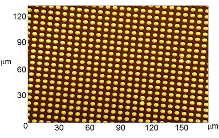
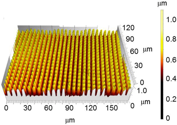
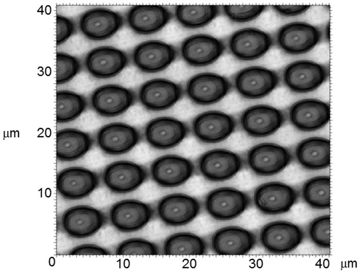
Fig. 2: Imaging methods for characterization of the nano- and micro-structured SWNT-PS films on Si: Leica DCM8 confocal microscope images of a micro-structured SWNT-PS film on Si in 2D (A) and the 3D topography (B) where the heights are indicated with a false color scale; and a Leica DCM8 "brightfield" image (C) of a micro-structured SWNT-PS film.
Electrical properties
Electrical conductivity of the SWNT-PS and SWNT-P3HT thin films on Si was measured with the sample placed between 2 electrodes [1, 2]. A sweeping voltage was applied between the top and bottom of the SWNT-P3HT film, and the resulting current was recorded as a current-voltage (I–V) curve. Results are shown in Figure 3. Measurements were repeated in 3 different locations on the sample up to 10 times in each location. The I–V curves showed good reproducibility.
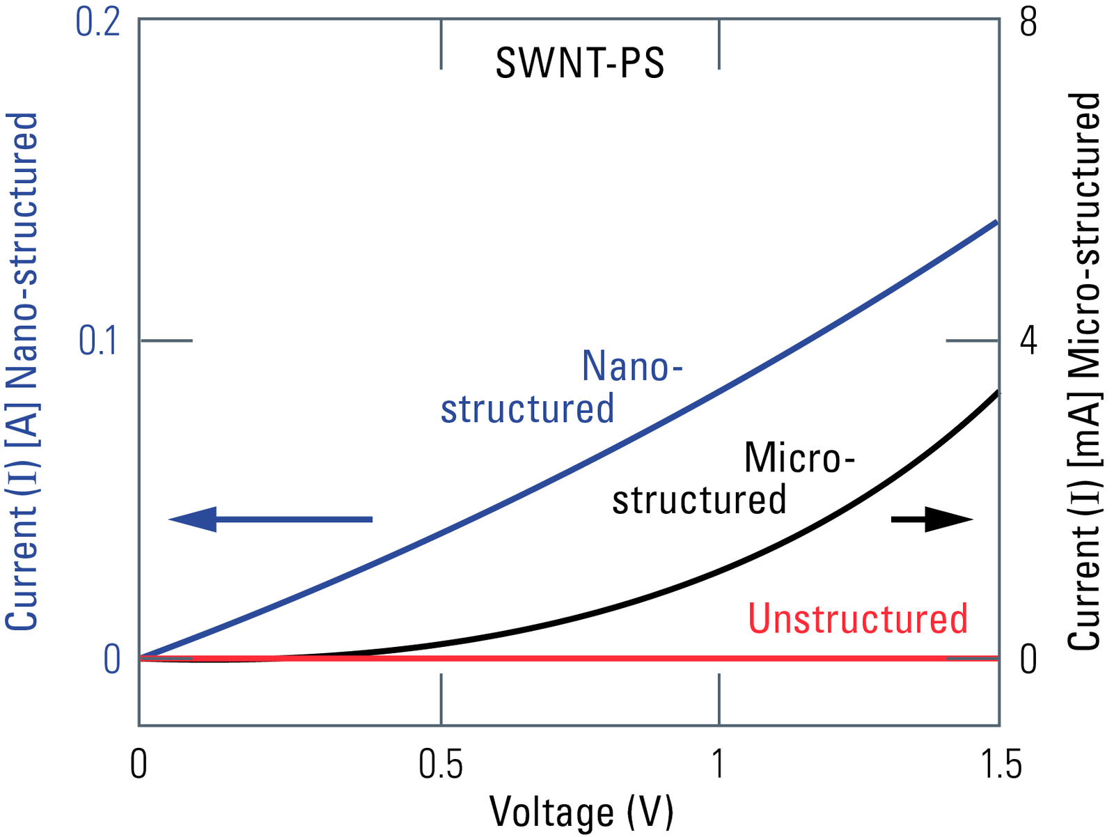
Fig. 3: Current vs. voltage (I–V) curves for nano-structured (nanoscale networks), micro-structured (microscale networks), and unstructured (random networks) SWNT-PS films on Si [2].
Overview of results
Nano-structured SWNT-PS samples versus micro-structured and unstructured
Results show that the conductivity or charge transfer of the nano- and micro-structured SWNT-PS samples is up to 100 million (108) times greater than that of the unstructured (random networks) SWNT-PS samples, where all samples contain similar concentrations of nanotubes [2]. From Figure 3, it can be seen that the nano-structured SWNT-PS samples have a conductivity nearly 100 times greater than that of the micro-structured SWNT-PS samples. Because of their higher conductivity and charge transfer, further discussion of the results here will focus on the nano-structured SWNT-polymer samples.
The charge transport mechanism is very different in the two types of networks, with the structured networks producing ohmic conduction and high conductivity at all concentrations and even low voltages. A high nanotube loading had been previously seen as the most important parameter for efficient charge transport and high conductivity in SWNT-polymer composites. These results show that the interconnectivity of the nanotubes inside the composite is the main factor influencing charge transport. In fact, high nanotube loads in unstructured samples with random networks still produce less efficient conduction pathways than nano- or micro-structured samples with much lower nanotube concentrations. Unstructured samples require much higher nanotube concentrations in order to render the composite conductive. The high nanotube concentration has the disadvantage of greater material costs for film production and increased probability of creating aggregates or bundles which can decrease charge transport and lower the device performance [2].
Conductivity of nano-structured and unstructured SWNT-P3HT films versus nanotube concentration
Measurements on samples with a large variation in the nanotube concentration show that efficient charge transport occurs at all concentrations, even at very low nanotube loading, much below the percolation threshold (≈ 2–3 wt%) typically reported for P3HT.
By increasing the interconnectivity of the tubes inside the nanoscale networks, the concentration required to form efficient charge transfer pathways was greatly reduced being much below the percolation threshold.
The dependence of the electrical current density, J, on the conductivity, σ, is given by Ohm’s law:
and from this equation an expression for the conductivity can be found:

where E is the electric field, R is the electrical resistance of the film, I is the measured current, V is the applied voltage, t is the sample thickness, and A is the sample/electrode contact area through which the current flows. Conductivity for the samples were calculated using experimentally obtained data and the expression above. Figure 4 below shows that the conductivity in the unstructured samples with random networks stays nearly the same, approximately the value for pure P3HT, at all concentrations (0.03, 0.12, 0.48, and 1.5 wt%) below 3 wt%, the percolation threshold for SWNT-P3HT. The nano-structured SWNT-P3HT samples consistently are much more conductive than the unstructured ones, even at very low nanotube concentrations. Thus, by increasing the interconnectivity of the nanotubes via nano-structuring, efficient charge transport pathways are able to be formed at low concentrations, much below the previously reported percolation threshold. A lower SWNT concentration reduces nanotube aggregation and can allow for a more economical means of large scale production for electronic applications, due to the high cost of nanotubes.
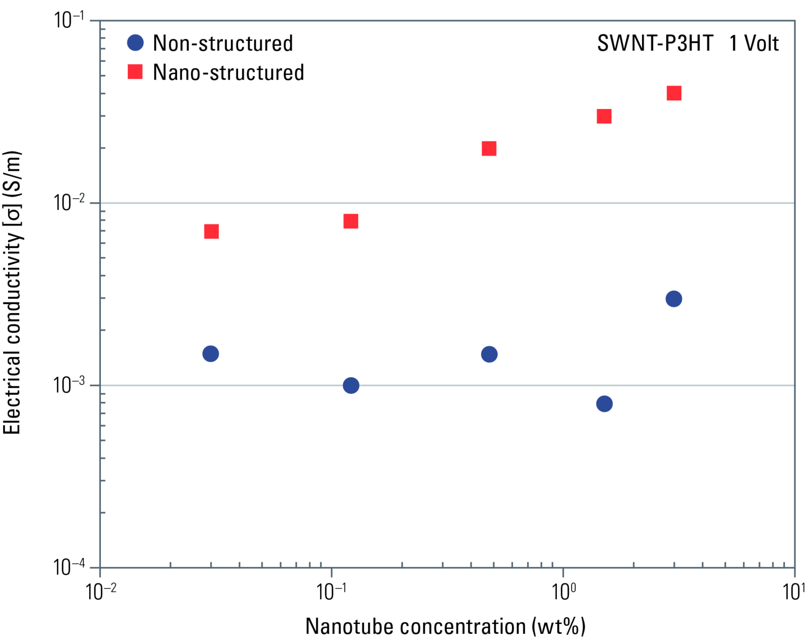
Fig. 4: Log-log plot of electrical conductivity, σ, of unstructured (random networks; blue) and nano-structured (nanoscale networks; red) SWNT-P3HT films measured at a voltage of 1 Volt versus the nanotube concentration in the film. The nanotube concentrations are 0.03, 0.12, 0.48, 1.5, and 3.0 wt%.
Electrical characteristics of nano-structured and unstructured SWNT-P3HT films
To understand better the electrical characteristics of the nano-structured and unstructured SWNT-P3HT films, the current density (J) can be measured as a function of the voltage (V). The obtained data can then be fitted to the power law:

where J is the measured current density and V is the applied voltage. For a log–log plot, the exponent a gives the slope of the line and log(b) is the y-intercept. A slope (a) close to 1 would indicate ohmic conduction. Previous work [1] has shown that log(J)–log(V) plots for the nano-structured films have a slope (a) between 1.0 and 1.1 for nanotube concentrations ranging from 0.03 to 3 wt%, indicating more ohmic conduction. By contrast, the unstructured films have a slope between 1.3 and 1.9 which indicates less ohmic conduction and less efficient charge transport.
Conduction in pure P3HT has been described as space-charge limited with the current density having a quadratic relation with the voltage (a = 2) [1]. The values of a for the unstructured SWNT-P3HT films (random networks) imply at least partially space-charge limited conduction, likely arising from poor interconnection between the nanotubes. The more ohmic conduction in the nano-structured SWNT-P3HT films with nanoscale networks can be explained by the formation of continuous paths with many nanotubes being highly interconnected [1].
Mechanism of formation of the nanoscale or microscale networks in nano- or micro-structured SWNT-polymer films
During the imprinting of the SWNT-polymer films, the nanotubes are forced into the cavities of the patterned mold by shear forces acting on the SWNT-polymer composite (refer to Figure 5) [1]. The nanotubes are first oriented in the plane of the substrate, a mainly 2D geometry, after spin coating. Afterwards, the second layer of pure polymer (P3HT or PS) is spun on top of the nanotubes. For nanotubes concentrations below the percolation threshold of 3 wt%, before imprinting the unstructured film's conductivity remains at values typical for the polymer (semiconducting P3HT, σ ≈ 10–3 S/m, or insulating PS). After imprinting and the formation of nano- or micro-structures (nanoscale or microscale SWNT networks) in the composite film, the conductivity increases up to 100 times in P3HT and up to 100 million times in PS [1, 2].

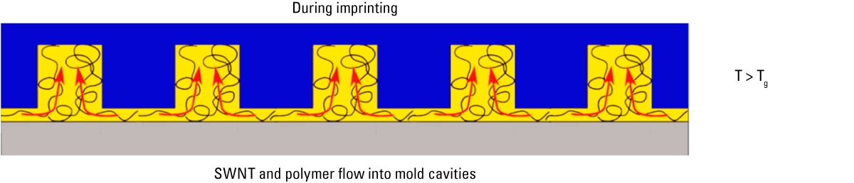
Fig. 5: Mechanism of nanoscale or microscale interconnected nanotube network formation due to imprinting. A) Unstructured, 2-layer SWNT-polymer composite film just before imprinting: the mold with cavities, film, and substrate are at a temperature (T) greater than the glass transition temperature (Tg) of the SWNT-polymer composite. B) SWNT-polymer film during imprinting where the mold is pressed onto the film and nanoscale or microscale interconnected nanotube networks are formed. The arrows denote flow of the nanotubes and polymer into the mold's cavities.
The dramatic increase in film conductivity after imprinting (formation of nanoscale or microscale networks) clearly indicates that the nanotubes change from a more planar to a more vertical orientation. This re-orientation of the nanotubes is most likely caused by the flow of the melted polymer into the cavities of the mold. The nanotubes appear to be dragged along with the flowing soft polymer at high temperature and this phenomenon enables more efficient conducting pathways to form across the film thickness compared to unstructured films.
Summary
Polymer composites with carbon nanotubes have become more and more interesting over the last decade, as they exhibit high performance in terms of mechanical and electrical properties. More recently, nanotube-polymer composites with high conductivity have been developed which have gained interest for optoelectronic applications.
Here it is shown that nanoscale and microscale patterning of films made from a polymer composite containing single wall carbon nanotubes (SWNTs) dramatically improves their electrical performance, i.e. conductivity. Both nano-structuring and micro-structuring of SWNT-polymer composites with this method of imprinting yields aligned and largely-interconnected SWNT networks. The interconnected SWNT networks significantly enhance charge transport across the film thickness compared to unstructured films with random, disconnected networks. The nano- or micro-structured SWNT-polymer films, with nanoscale or microscale nanotube networks, show higher conductivity than unstructured SWNT-polymer films with random networks at all nanotube concentrations, especially below the percolation threshold.
This novel approach utilizing imprinting allows nano-structured or micro-structured nanotube-polymer composite films with interconnected nanoscale or microscale nanotube networks to be created. The nanoscale or microscale nanotube networks give the films enhanced electrical properties, such as conductivity. The method can be applied for large scale production of nanotube-polymer composite films using large area imprinting and roll-to-roll processes. These results should make this nano-/micro-engineering technique very appealing for hybrid and organic photovoltaic devices, such as solar cells.
References
- Boulanger N, Yu J, and Barbero DR: SWNT nano-engineered networks strongly increase charge transport in P3HT. Nanoscale 6 (20): 11491–12158 (2014); dx.doi.org/10.1039/c4nr01542h.
- Boulanger N, Barbero DR: Nanostructured networks of single wall carbon nanotubes for highly transparent, conductive, and anti-reflective flexible electrodes. Applied Physics Letters 103 (2): 1–5 (2013); dx.doi.org/10.1063/1.4813498.
- Barbero DR, Boulanger N, Ramstedt M, and Yu J: Nano-Engineering of SWNT Networks for Enhanced Charge Transport at Ultralow Nanotube Loading. Advanced Materials 26: 3111–17 (2014); dx.doi.org/10.1002/adma.201305843.
- Wikipedia: Percolation threshold.
- Wikipedia: Glass transition.