Leica EM TIC 3X
イオンビームミリング
電顕用試料作製装置
製品紹介
Home
Leica Microsystems
Leica EM TIC 3X Ion Beam Milling System
加工効率と柔軟性
最新の記事を読む

Cross-section Analysis for Electronics Manufacturing
This article describes cross-section analysis for electronics concerning quality control and failure analysis of printed circuit boards (PCBs) and assemblies (PCBAs), integrated circuits (ICs), etc.
 chip cross section acquired at higher magnification showing a region of interest.")
Structural and Chemical Analysis of IC-Chip Cross Sections
This article shows how electronic IC-chip cross sections can be efficiently and reliably prepared and then analyzed, both visually and chemically at the microscale, with the EM TXP and DM6 M LIBS…
. The grains are highlighted with arbitrary colors.")
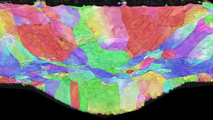
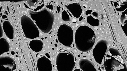
High-Quality EBSD Sample Preparation
This article describes a method for EBSD sample preparation of challenging materials. The high-quality samples required for electron backscatter diffraction are prepared with broad ion-beam milling.

Cross Section Ion Beam Milling of Battery Components
Sample Preparation of Lithium battery systems requires high quality surface preparation to evaluate their internal structure and morphology. Due to the brittle materials involved, preparing pristine…

Download EM Workflow Solutions Booklet
This publication is a compilation of appropriate workflows for the most frequently used sample preparation methods, like Correlative Methodologies, Optogenetics & Electro-Physiology, Surface Analysis,…
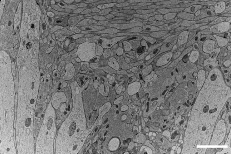
Exploring the Structure and Life Cycle of Viruses
The SARS-CoV-2 outbreak started in late December 2019 and has since reached a global pandemic, leading to a worldwide battle against COVID-19. The ever-evolving electron microscopy methods offer a…

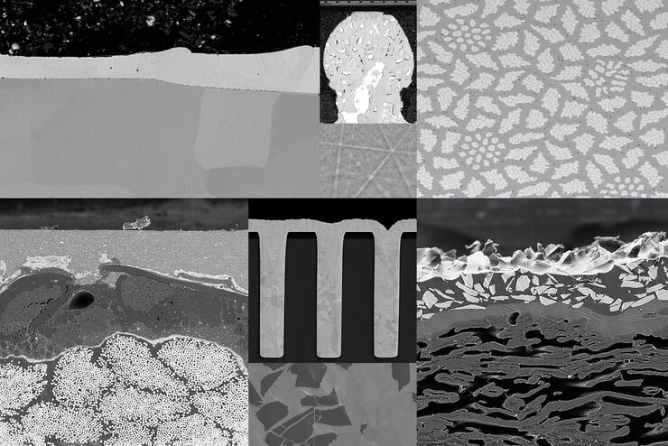
Application Booklet for EM TIC 3X
Today, ion beam milling is one of the most widely-used methods for preparing samples for electron microscopy. Download this 76-pages booklet today and learn how to improve your processes.
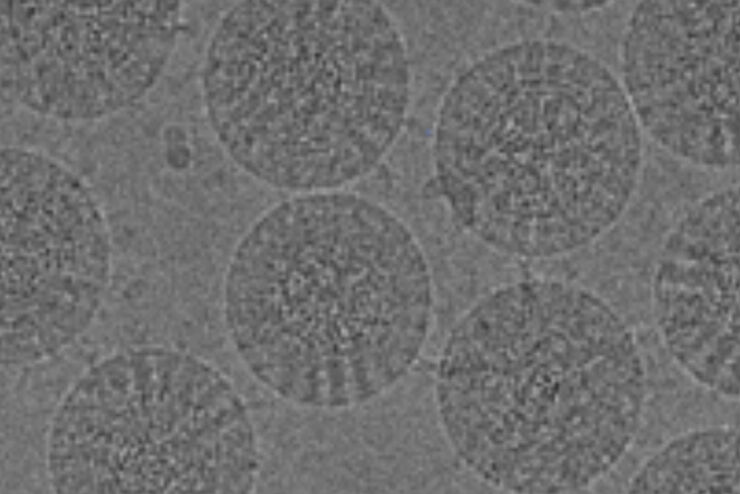
Workflows and Instrumentation for Cryo-electron Microscopy
Cryo-electron microscopy is an increasingly popular modality to study the structures of macromolecular complexes and has enabled numerous new insights in cell biology. In recent years, cryo-electron…
Introduction to Ion Beam Etching with the EM TIC 3X
In this article you can learn how to optimize the preparation quality of your samples by using the ion beam etching method with the EM TIC 3X ion beam milling machine. A short introduction of the…
Workflow Solutions for Sample Preparation Methods for Material Science
This brochure presents and explains appropriate workflow solutions for the most frequently required sample preparation methods for material science samples.
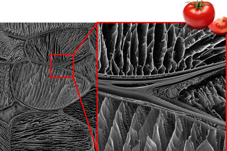
Studying the Microstructure of Natural Polymers in Fine Detail
The potential of cryogenic broad ion beam milling used in combination with scanning electron microscopy (cryo-BIB-SEM) for imaging and analyzing the microstructure of cryogenically stabilized soft…
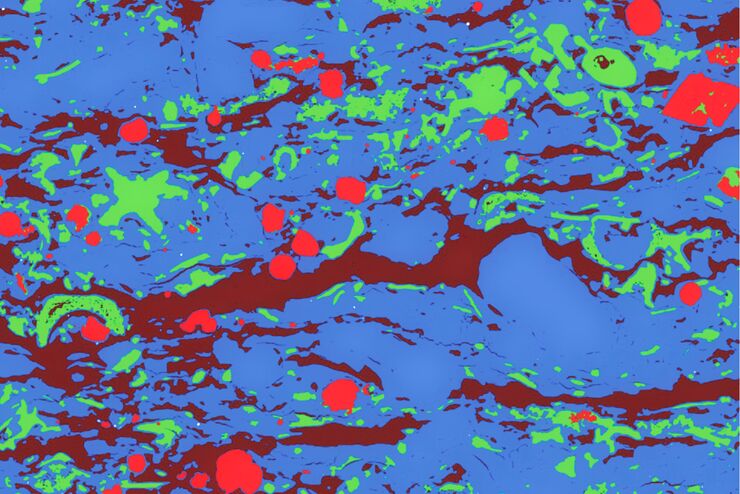
Macroscale to Nanoscale Pore Analysis of Shale and Carbonate Rocks
Physical porosity in rocks, like shale and carbonate, has a large effect on the their storage capacity. The pore geometries also affect their permeability. Imaging the visible pore space provides…
Practical Applications of Broad Ion Beam Milling
Mechanical polishing can be time consuming and frustrating. It can also introduce unwanted artifacts when preparing cross-sectioned samples for electron backscatter diffraction (EBSD) in the scanning…
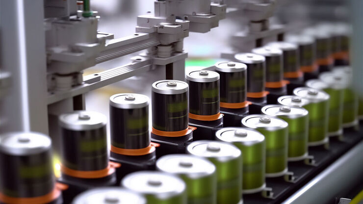
Battery Manufacturing
Battery manufacturing has several key challenges concerning inspection. Solutions for sample preparation and microscopic visual and chemical analysis are needed.
応用分野
自動車&輸送機器業界
ライカのインテリジェントなイメージングソリューションは、現在および将来のニーズに対応し、お客様は技術革新に集中することができます。
工業用光学顕微鏡
材料解析には、金属合金、半導体、ガラス、セラミック、プラスチック、ポリマーなど、さまざまな材料の画像処理、測定、分析のための顕微鏡ソリューションが必要です。
工業用顕微鏡のマーケット
稼働時間を最大化し、生産性向上により、お客様の収益に貢献します。ライカの顕微鏡(マイクロスコープ)ソリューションは、微細な異物や残渣なども見逃しなく、迅速かつ信頼性の高い分析、文書化、結果報告を実現します。ライカマイクロシステムズは、幅広いソリューションとエキスパートによるサポートを提供し、さまざまなアプリケーションのニーズにお応えします。
エレクトロニクスのための断面解析
電子・エレクトロニクス業界では、断面解析により、プリント基板(PCB)、アセンブリ(PCBA)、集積回路(IC)などのコンポーネントの故障メカニズムを詳細に解析します。
エレクトロニクスおよび半導体産業
電子機器や半導体にとって、PCB、ウェハー、ICチップ、バッテリーの効率的な検査、断面解析、清浄度分析、研究開発を可能にするソリューションは極めて重要です。

もっと知りたいですか?
お気軽にお問合せください
ライカまでお気軽にご相談ください Show local contacts