Leica EM TIC 3X
Sistema de fresamento de feixes de íon
Preparação de amostra para microscopia eletrônica
Produtos
Página inicial
Leica Microsystems
Leica EM TIC 3X Sistema de fresamento de feixes de íon
Eficiência e flexibilidade
Leia os nossos artigos mais recentes

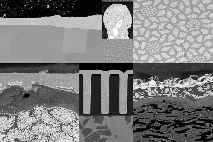
Cross-section Analysis for Electronics Manufacturing
This article describes cross-section analysis for electronics concerning quality control and failure analysis of printed circuit boards (PCBs) and assemblies (PCBAs), integrated circuits (ICs), etc.
 chip cross section acquired at higher magnification showing a region of interest.")
Structural and Chemical Analysis of IC-Chip Cross Sections
This article shows how electronic IC-chip cross sections can be efficiently and reliably prepared and then analyzed, both visually and chemically at the microscale, with the EM TXP and DM6 M LIBS…
. The grains are highlighted with arbitrary colors.")
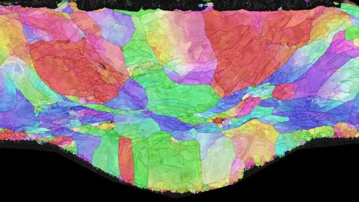
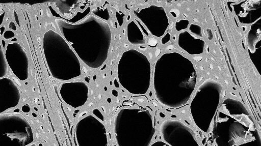
High-Quality EBSD Sample Preparation
This article describes a method for EBSD sample preparation of challenging materials. The high-quality samples required for electron backscatter diffraction are prepared with broad ion-beam milling.

Cross Section Ion Beam Milling of Battery Components
Sample Preparation of Lithium battery systems requires high quality surface preparation to evaluate their internal structure and morphology. Due to the brittle materials involved, preparing pristine…

Download EM Workflow Solutions Booklet
This publication is a compilation of appropriate workflows for the most frequently used sample preparation methods, like Correlative Methodologies, Optogenetics & Electro-Physiology, Surface Analysis,…
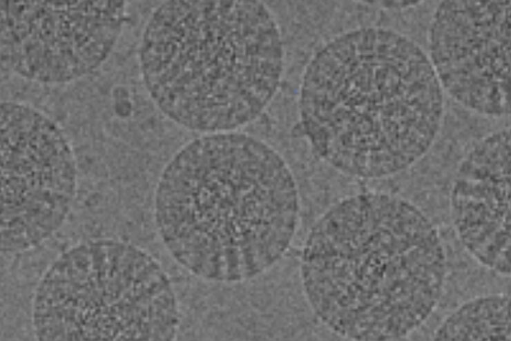
Exploring the Structure and Life Cycle of Viruses
The SARS-CoV-2 outbreak started in late December 2019 and has since reached a global pandemic, leading to a worldwide battle against COVID-19. The ever-evolving electron microscopy methods offer a…

Application Booklet for EM TIC 3X
Today, ion beam milling is one of the most widely-used methods for preparing samples for electron microscopy. Download this 76-pages booklet today and learn how to improve your processes.
Workflows and Instrumentation for Cryo-electron Microscopy
Cryo-electron microscopy is an increasingly popular modality to study the structures of macromolecular complexes and has enabled numerous new insights in cell biology. In recent years, cryo-electron…
Introduction to Ion Beam Etching with the EM TIC 3X
In this article you can learn how to optimize the preparation quality of your samples by using the ion beam etching method with the EM TIC 3X ion beam milling machine. A short introduction of the…
Workflow Solutions for Sample Preparation Methods for Material Science
This brochure presents and explains appropriate workflow solutions for the most frequently required sample preparation methods for material science samples.
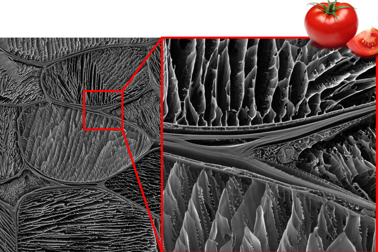
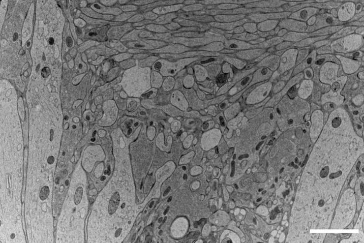
Studying the Microstructure of Natural Polymers in Fine Detail
The potential of cryogenic broad ion beam milling used in combination with scanning electron microscopy (cryo-BIB-SEM) for imaging and analyzing the microstructure of cryogenically stabilized soft…
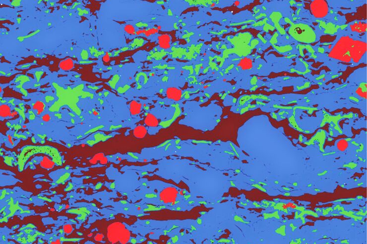
Macroscale to Nanoscale Pore Analysis of Shale and Carbonate Rocks
Physical porosity in rocks, like shale and carbonate, has a large effect on the their storage capacity. The pore geometries also affect their permeability. Imaging the visible pore space provides…
Practical Applications of Broad Ion Beam Milling
Mechanical polishing can be time consuming and frustrating. It can also introduce unwanted artifacts when preparing cross-sectioned samples for electron backscatter diffraction (EBSD) in the scanning…
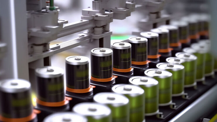
Battery Manufacturing
Battery manufacturing has several key challenges concerning inspection. Solutions for sample preparation and microscopic visual and chemical analysis are needed.
Campos de aplicação
Automotivo e transporte microscópios
Nós, aqui na Leica, desejamos ser seu colaborador com o qual pode confiar, a fim de orientá-lo quanto às soluções ideais em captura e processamento de imagens, para que você possa estar à frente da…
Microscópios de análise de materiais
A análise de materiais requer soluções de microscopia para a aquisição de imagens, medição e análise de recursos em diversos materiais, como ligas metálicas, semicondutores, vidro e cerâmica, bem como…
Mercados de microscopia industrial
Maximizar o tempo de atividade e atingir as metas de forma eficiente ajuda seu resultado final. As soluções de microscópio Leica podem fornecer uma visão dos menores detalhes da amostra, bem como…
Análise de cortes transversais para componentes eletrônicos
A análise de cortes transversais para componentes eletrônicos permite uma análise detalhada dos mecanismos de falha de componentes, como placas de circuito impresso (PCBs), conjuntos (PCBAs) e…
Indústria de eletrônicos e semicondutores
Para eletrônicos e semicondutores, soluções que permitem a inspeção eficiente, análise de seção transversal e limpeza, além da P&D de PCBs, wafers, chips IC e baterias são cruciais.

Interessado em saber mais?
Fale com nossos especialistas.
Você prefere consultoria pessoal? Show local contacts