
Science Lab
Science Lab
The knowledge portal of Leica Microsystems offers scientific research and teaching material on the subjects of microscopy. The content is designed to support beginners, experienced practitioners and scientists alike in their everyday work and experiments. Explore interactive tutorials and application notes, discover the basics of microscopy as well as high-end technologies – become part of the Science Lab community and share your expertise!
Filter articles
Tags
Story Type
Products
Loading...
 at the edge of a battery electrode acquired with a DVM6 digital microscope.")
Burr Detection During Battery Manufacturing
See how optical microscopy can be used for burr detection on battery electrodes and determination of damage potential to achieve rapid and reliable quality control during battery manufacturing.
Loading...
 and oblique (right) brightfield illumination using a Leica compound microscope. The defect on the wafer surface is clearly more visible with oblique illumination.")
Rapid Semiconductor Inspection with Microscope Contrast Methods
Semiconductor inspection for QC of materials like wafers can be challenging. Microscope solutions that offer several contrast methods enable fast and reliable defect detection and efficient workflows.
Loading...

How to Boost your Microelectronic Component Inspection Performance
Do you need to see more when inspecting silicon wafers or MEMS? Would you like to get sharp and detailed sample images which are similar to those from electron microscopes?
Watch this free webinar…
Loading...
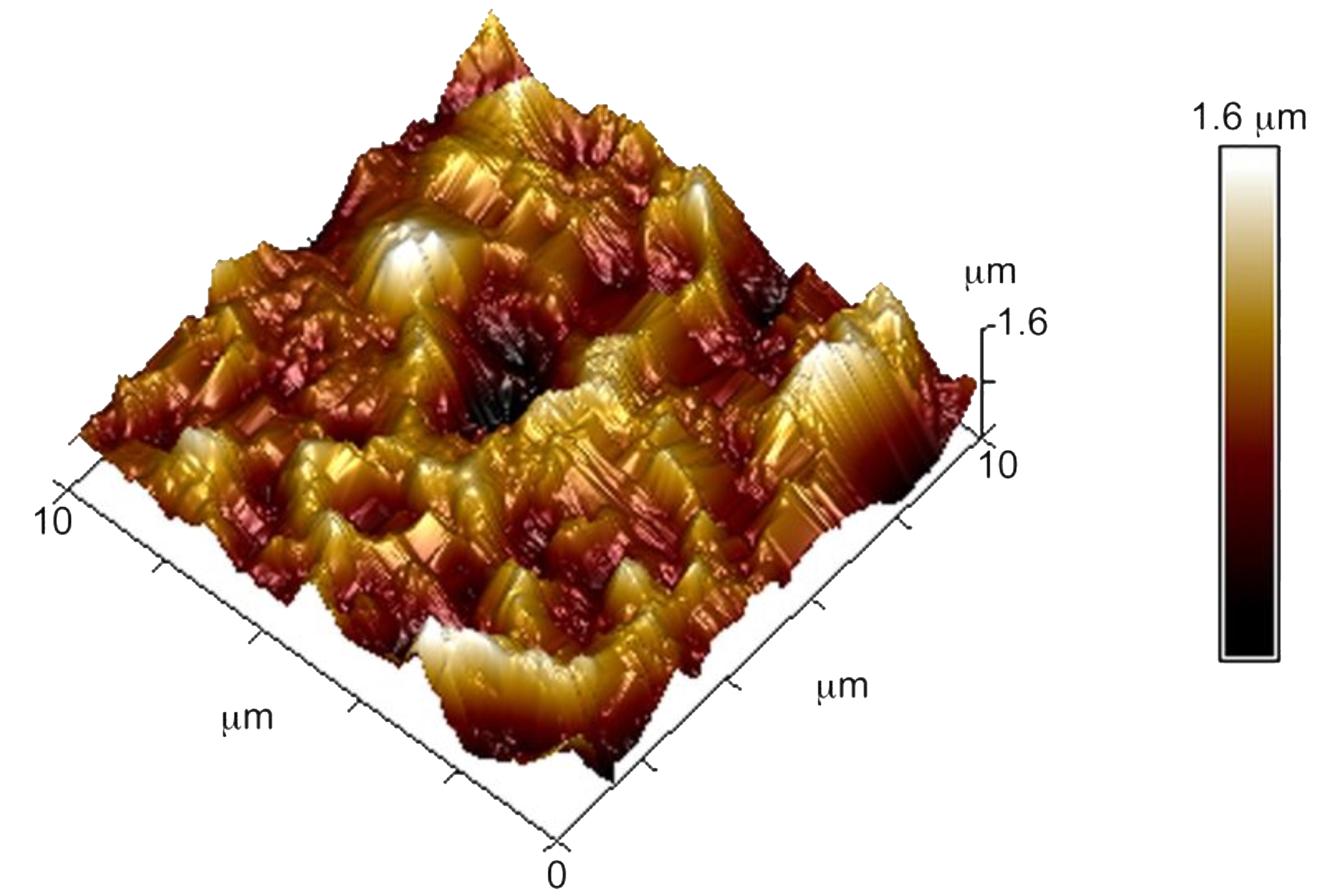
Brief Introduction to Surface Metrology
This report briefly discusses several important metrology techniques and standard definitions commonly used to assess the topography of surfaces, also known as surface texture or surface finish. With…