
Science Lab
Science Lab
The knowledge portal of Leica Microsystems offers scientific research and teaching material on the subjects of microscopy. The content is designed to support beginners, experienced practitioners and scientists alike in their everyday work and experiments. Explore interactive tutorials and application notes, discover the basics of microscopy as well as high-end technologies – become part of the Science Lab community and share your expertise!
Filter articles
Tags
Story Type
Products
Loading...
 at the edge of a battery electrode acquired with a DVM6 digital microscope.")
Burr Detection During Battery Manufacturing
See how optical microscopy can be used for burr detection on battery electrodes and determination of damage potential to achieve rapid and reliable quality control during battery manufacturing.
Loading...

Battery Particle Detection During the Production Process
How battery particle detection and analysis is enhanced with optical microscopy and laser spectroscopy for rapid, reliable, and cost-effective QC during battery production is explained in this…
Loading...

Key Factors for Efficient Cleanliness Analysis
An overview of the key factors necessary for technical cleanliness and efficient cleanliness analysis concerning automotive and electronics manufacturing and production is provided in this article.
Loading...
 and oblique (right) brightfield illumination using a Leica compound microscope. The defect on the wafer surface is clearly more visible with oblique illumination.")
Rapid Semiconductor Inspection with Microscope Contrast Methods
Semiconductor inspection for QC of materials like wafers can be challenging. Microscope solutions that offer several contrast methods enable fast and reliable defect detection and efficient workflows.
Loading...

Cross-section Analysis for Electronics Manufacturing
This article describes cross-section analysis for electronics concerning quality control and failure analysis of printed circuit boards (PCBs) and assemblies (PCBAs), integrated circuits (ICs), etc.
Loading...
 chip cross section acquired at higher magnification showing a region of interest.")
Structural and Chemical Analysis of IC-Chip Cross Sections
This article shows how electronic IC-chip cross sections can be efficiently and reliably prepared and then analyzed, both visually and chemically at the microscale, with the EM TXP and DM6 M LIBS…
Loading...

Key Factors to Consider When Selecting a Stereo Microscope
This article explains key factors that help users determine which stereo microscope solution can best meet their needs, depending on the application.
Loading...
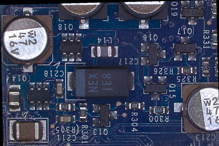
Rapid and Reliable Examination of PCBs & PCBAs with Digital Microscopy
Digital microscopes provide users with a convenient and rapid way to acquire high-quality, reliable image data and make quick inspection and analysis of printed circuit boards (PCBs) and assemblies…
Loading...

What is the FusionOptics Technology?
Leica stereo microscopes with FusionOptics provide optimal 3D perception. The brain merges two images, one with large depth of field and the other with high resolution, into one 3D image.