
Microscope and Sample-Preparation Solutions for Electronics Industry
Perform reliable and efficient inspection during production and development of electronic and semiconductor components according to your needs with Leica microscope and sample-preparation solutions.
Stay ahead of the competition when developing cutting-edge technology and components. You can optimize your workflows and production to keep them cost-effective.
AREAS OF EXPERTISE
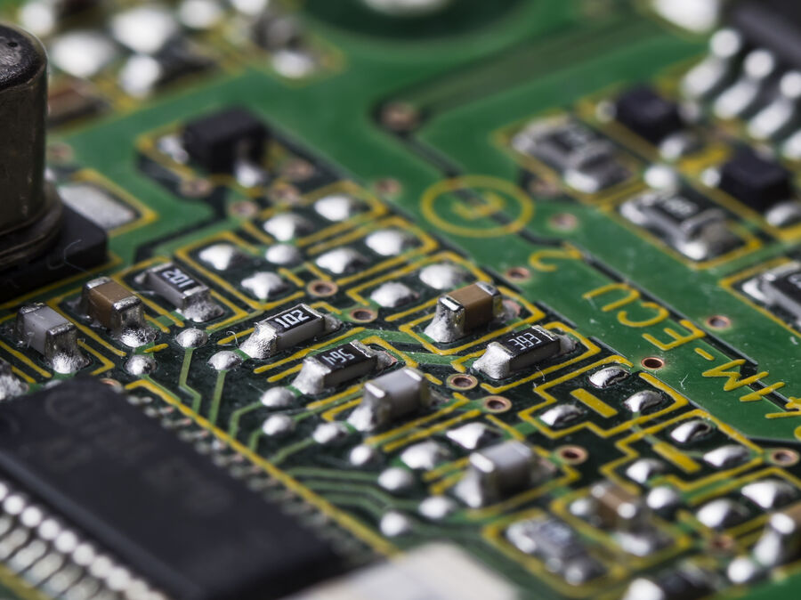
PCBs/PCBAs (printed-circuit boards and assemblies)
Identify defects in terms of soldering, leads, and component contacts, as well as the presence of potentially damaging particles and other types of contamination to ensure optimal performance and lifetime.
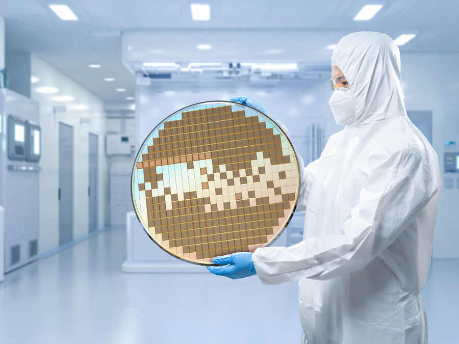
Semiconductors
Achieve fast and precise inspection and analysis for wafer processing, as well as IC packaging, assembly, and testing to ensure the quality and reliability of IC chips and other semiconductor components.

Cross sections of electronic components
Optimize your sample preparation and cross-section analysis of electronic components, e.g., PCBs, PCBAs, and integrated circuits (ICs). Evaluate efficiently the microstructure and identify quickly defects during cross-section analysis.
For efficient inspection, quality control (QC), failure analysis, and research & development (R&D), including cross-section and cleanliness analysis, Leica solutions can help you meet your application needs for sample preparation and microscopic analysis.
Leica Solutions
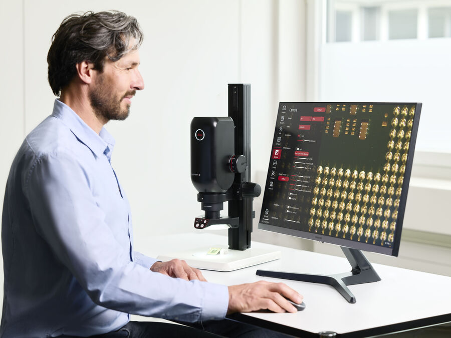
Emspira 3 Digital Microscope
Combines everything needed to perform comprehensive visual inspection into a single system, including comparison, measurement, and sharing of documentation.
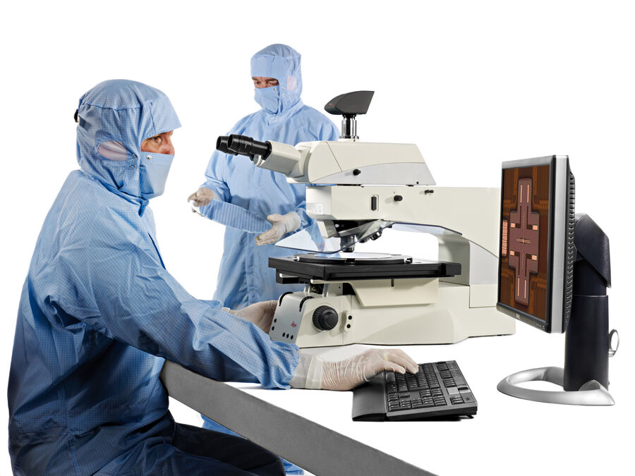
DM8000 M / DM12000 M Optical Inspection Systems
Speed up throughput when inspecting wafers with an 8’’/200 mm and 12”/300 mm diameter. With a single press of a button, you can change the magnification, illumination, or contrast mode.
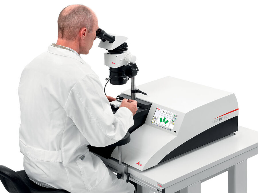
EM TIC 3X Ion Beam Milling System
Allows sample preparation of high-quality cross sections and planar surfaces for scanning electron microscopy (SEM), atomic force microscopy (AFM), and microstructure analysis. The internal structure of the sample is revealed. Preparation of many materials can be done at room or cryo temperatures.
* Terms and Conditions
- This promotion is only open to new Leica customers (no order placed in the last 3 years).
- Offer expires June 30th 2025 and can be applied to orders placed up until this date.
- This offer cannot be used in conjunction with any other promotion or discount, is subject to availability and may be withdrawn at any time.
- Valid for the following countries: Austria, Germany, Switzerland, Belgium, Luxembourg, Spain, Italy, Portugal, the Netherlands, United Kingdom & France.
- For all other countries in the EMEA region: Please check with your local Leica partner about the availability of this promotion.
