연락처
전자 장치의 단면 분석

전자 장치의 단면 분석

전자 장치의 단면 분석을 통해 인쇄 회로 기판(PCB), 조립품(PCBA) 및 집적 회로(IC)와 같은 전자 부품의 내부 미세 구조를 검사할 수 있습니다. 이러한 부품은 종종 불투명한 재질로 만들어집니다. 단면 분석을 위해, 부품의 단면을 만들고 광학현미경, 전자 현미경, 분광법으로 분석함해서 입자, 위상, 층, 계면, 균열, 공극, 결함 등의 구조와 조성을 밝혀냅니다. 단면 분석은 PCB, PCBA, IC 및 기타 전자 부품의 품질 관리(QC), 고장 분석(FA), 연구 개발(R&D)에 유용합니다.

도움이 필요하십니까?

필요 사항과 예산에 맞는 단면 분석에 대해 전문가의 조언이 필요하다면 현지 이미징 전문가와 상담해 보세요.

단면 분석은 PCB, PCBA, IC 및 기타 전자 부품의 품질 관리(QC), 고장 분석(FA), 연구 개발(R&D)에 유용합니다.

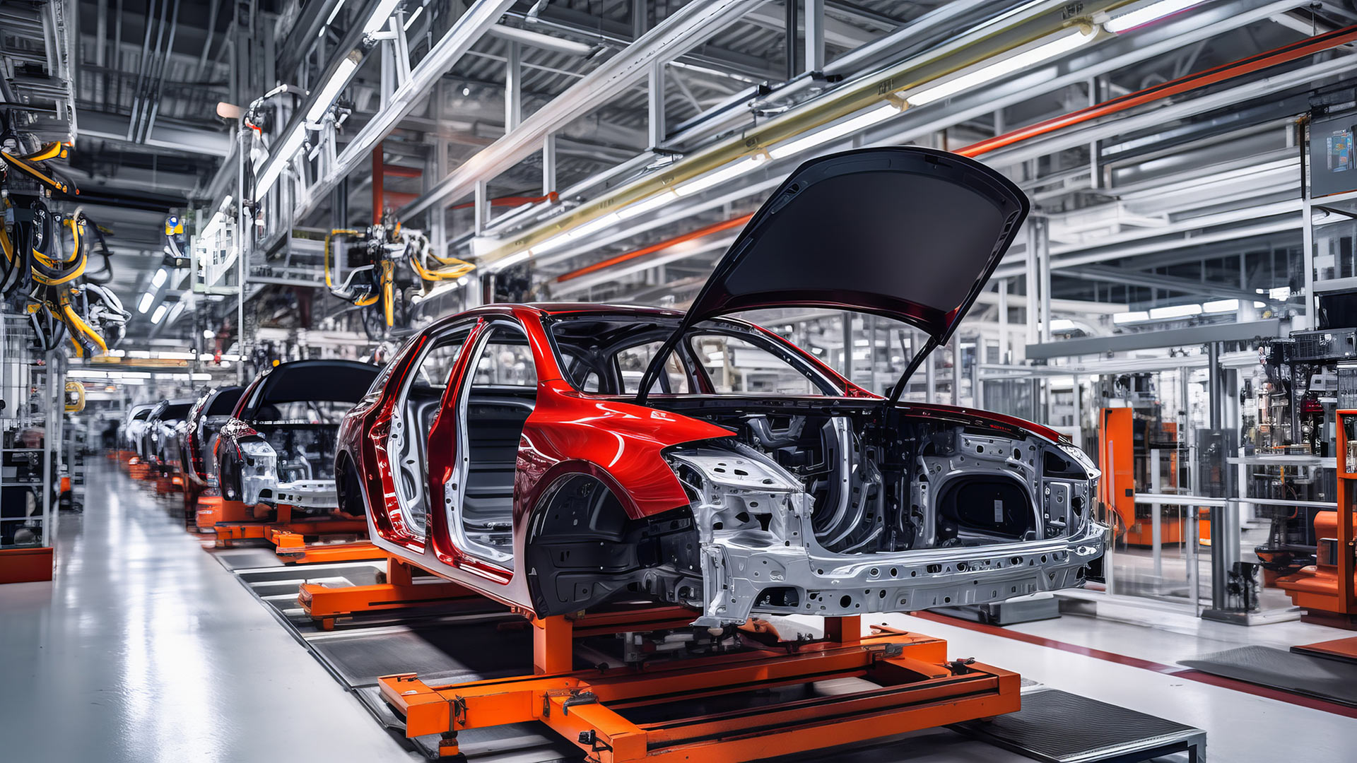
제조업에서 말하는 단면이란 무엇입니까?

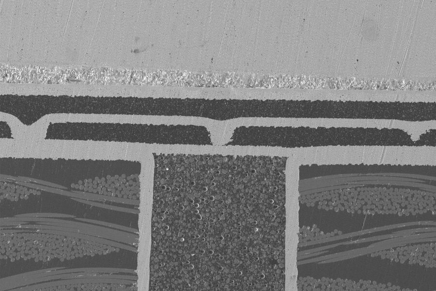
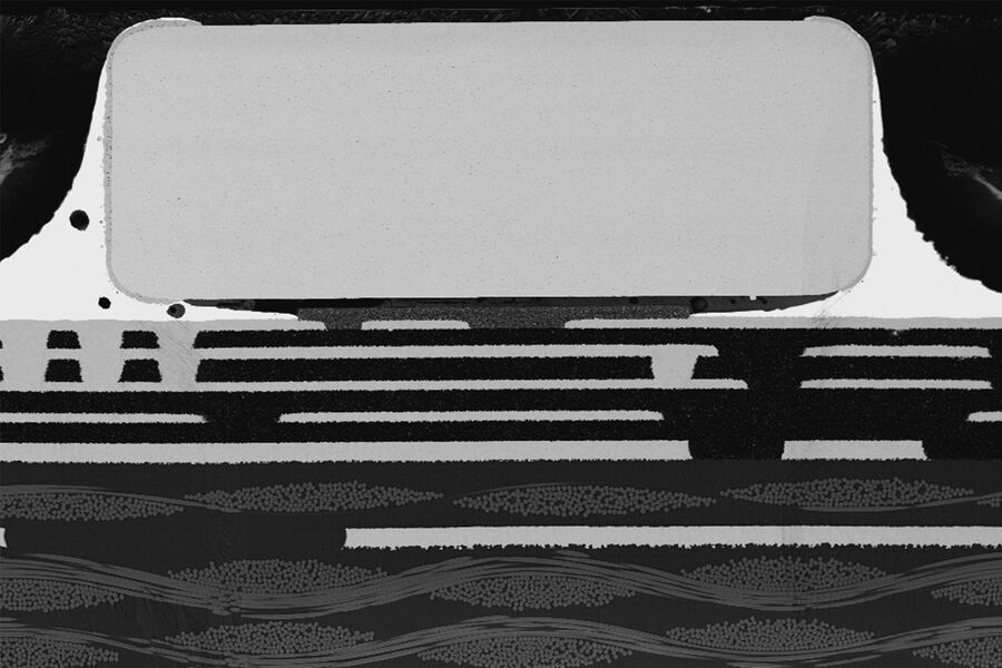
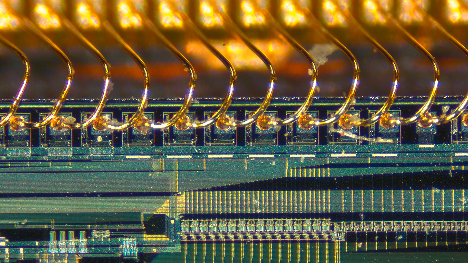
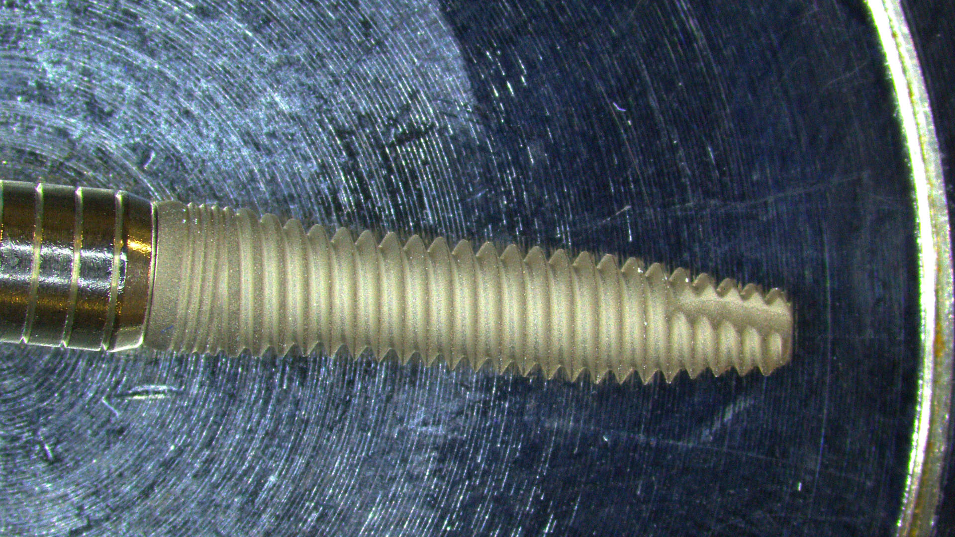
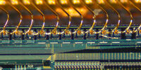
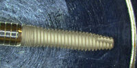
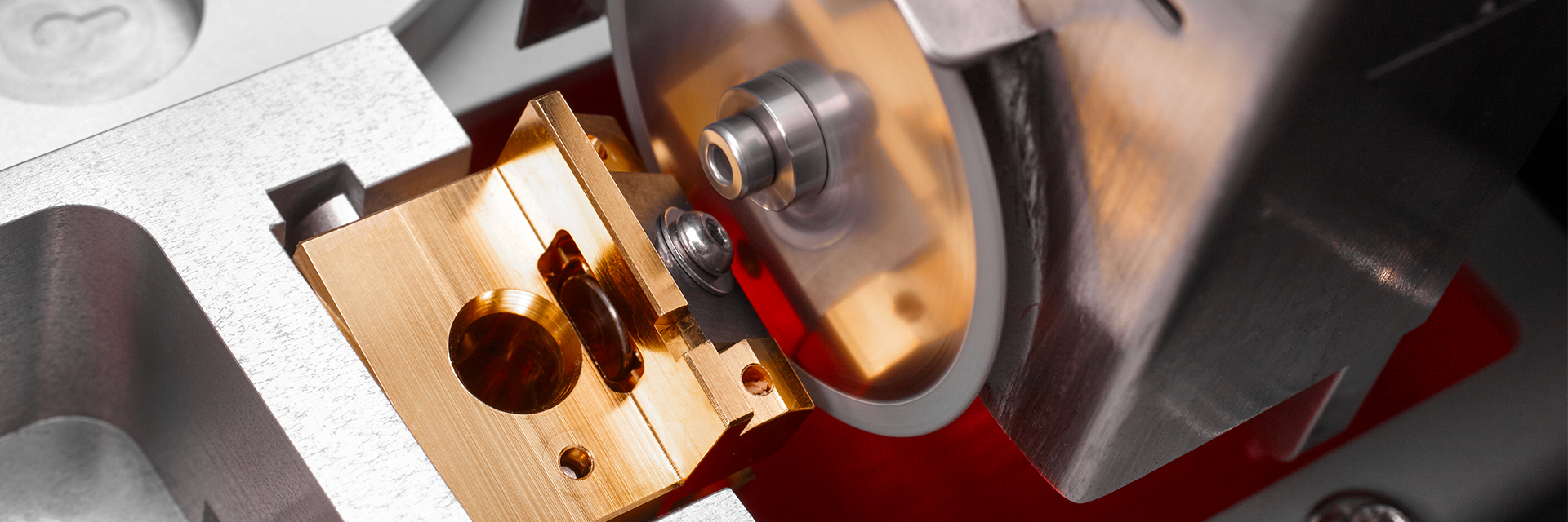
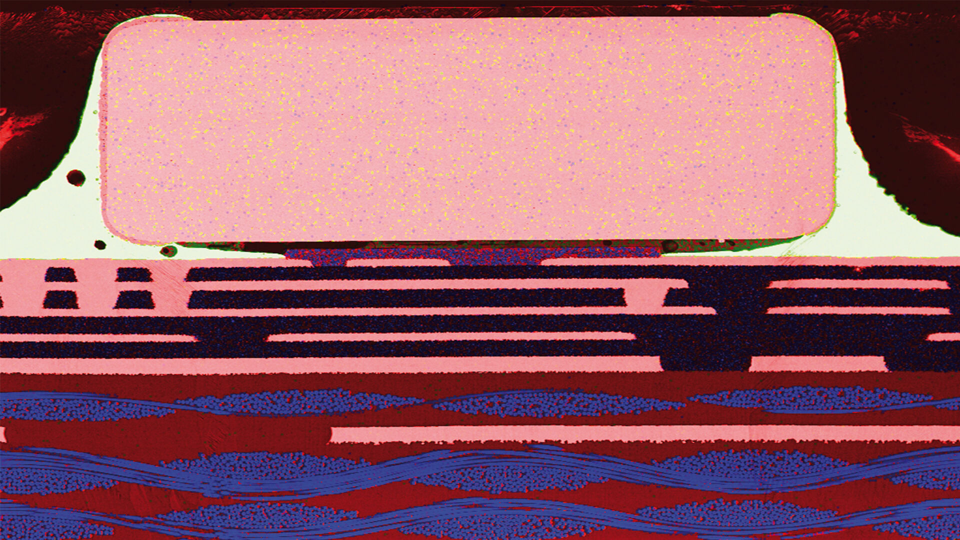
금속 합금, 세라믹, 인쇄 회로 기판(PCB), 조립품(PCBA) 또는 집적 회로(IC)와 같은 재료의 단면 절단을 위해, 그 부피를 특정 방향으로 가로질러 잘라서 얇은 조각으로 만들어서 벌크를 드러나게 합니다. 그러면 내부 미세 구조를 관찰할 수 있습니다. PCB 및 IC의 경우 단면을 절단하면 품질 관리 및 고장 분석에 유용합니다.

재료 또는 제품의 단면이란 무엇입니까?

단면은 내부 구조를 검사할 수 있는 금속, 세라믹, 고분자, 복합 재료, 광물, 회로판 또는 집적 회로와 같은 재료 또는 제품의 일부분입니다. 재료 또는 제품의 시료를 특정 방향 축을 따라 절단한 다음 갈고 연마해서 매끄럽고 평평한 표면을 만듭니다. 이 분석은 종종 광학현미경이나 전자 현미경 또는 분광법을 사용하여 수행됩니다.

단면 절단의 목적은 무엇입니까?

단면 절단은 품질 관리 및 고장 분석에 매우 유용합니다. 인쇄 회로 기판(PCB) 및 조립품(PCBA), 집적 회로(IC), 기판 재료 및 층, 상호 연결, 와이어 본드, 납땜 접합 및 캡슐화 재료와 같은 전자 부품의 구조적 무결성을 평가하는 데 사용됩니다. 단면 분석은 구성 부품 고장을 일으킬 수 있는 결함을 식별하는 데도 도움이 됩니다.

3개의 간단한 질문에 답하여 맞춤 해결책을 얻으세요.

특정한 요건에 맞는 전용 환경 설정을 이용할 수 있습니다. 간단한 설문에 답하고 요구 사항에 가장 알맞은 솔루션을 찾아보세요. 담당자와 상담을 원하시면 여기를 클릭하여 연락처를 입력해 주세요.

문의하기

{{ question.questionText }}

답을 선택해 주세요!

베스트 매치

{{ resultProduct.header }}

{{ resultProduct.subheader }}

{{ resultProduct.description }}

{{ resultProduct.features }}

정보 패키지 요청하기

문의하기

아래의 '지금 전송' 버튼 클릭함으로써 라이카마이크로시스템즈의 이용약관과 개인정보 취급방침 을 검토하고 동의하였음을 확인합니다. 또한 본인의 개인정보에 대한 선택을 라이카마이크로시스템즈의 개인정보 취급방침 에 따라 처리하는것에 동의합니다.

PCB/PCBA 단면 준비

PCB/PCBA 단면 준비는 여러 단계로 이루어집니다:

  • 선택한 영역에서 인쇄 회로 기판(PCB) 또는 조립품(PCBA)의 일부분을 잘라냅니다.
  • PCB/PCBA의 내부 미세 구조와 다른 층을 드러내기 위해 단면을 클리닝, 마운팅, 갈아내기, 연마, 이온 연마를 하고 때로는 에칭도 합니다.

그러면 광학(OM) 또는 전자 현미경(EM)으로 쉽게 관찰할 수 있는 매끄럽고 평평한 표면이 만들어집니다. OM 또는 EM을 사용한 검사를 통해 미세 구조 및 다양한 층을 검사할 수 있습니다.

IC 단면 준비

집적 회로(IC) 단면 준비는 다음이 필요합니다:

  1. 분석할 특정 영역 선택하고 잘라내기
  2. 캡슐화 재료 제거
  3. 에폭시 수지에 IC 시료 포매
  4. IC 내부 구조를 드러내기 위해 절단이나 이온 빔 연마로 얇은 조각으로 자르기
  5. 매끄러운 표면을 얻기 위한 갈기와 연마
  6. 특정 IC 구조를 드러내기 위해 선택적인 에칭을 사용할 수 있습니다
  7. 광학 현미경, 전자 현미경 및 분광법 (예: LIBS가 있는 복합 현미경 또는 EDS가 있는 SEM)으로 IC 단면을 시각화하고 분석해서 미세 정보와 내부 미세 구조를 파악합니다.

전자 장치의 단면 분석 관련 기사

전자 장치의 단면 분석에 관한 최신 기사 읽기

Leica Microsystems 지식 포털은 현미경에 관한 과학 연구 및 교육 자료를 제공합니다. 초보자와 숙련된 기술자, 과학자가 일상 업무와 실험에 모두 사용할 수 있는 콘텐츠로 구성되어 있습니다.

더 많은 기사
Image of burrs (red arrows) at the edge of a battery electrode acquired with a DVM6 digital microscope.

Burr Detection During Battery Manufacturing

See how optical microscopy can be used for burr detection on battery electrodes and determination of damage potential to achieve rapid and reliable quality control during battery manufacturing.
Particles observed on the surface of a particle trap which could be used for technical cleanliness during battery production.

Battery Particle Detection During the Production Process

How battery particle detection and analysis is enhanced with optical microscopy and laser spectroscopy for rapid, reliable, and cost-effective QC during battery production is explained in this…
Particulate contamination in between moving metal plates.

Key Factors for Efficient Cleanliness Analysis

An overview of the key factors necessary for technical cleanliness and efficient cleanliness analysis concerning automotive and electronics manufacturing and production is provided in this article.
Images of the same area of a processed wafer taken with standard (left) and oblique (right) brightfield illumination using a Leica compound microscope. The defect on the wafer surface is clearly more visible with oblique illumination.

Rapid Semiconductor Inspection with Microscope Contrast Methods

Semiconductor inspection for QC of materials like wafers can be challenging. Microscope solutions that offer several contrast methods enable fast and reliable defect detection and efficient workflows.
Preparation of an IC-chip cross section: grinding and polishing of the chip cross section.

Cross-section Analysis for Electronics Manufacturing

This article describes cross-section analysis for electronics concerning quality control and failure analysis of printed circuit boards (PCBs) and assemblies (PCBAs), integrated circuits (ICs), etc.
Image of an integrated-circuit (IC) chip cross section acquired at higher magnification showing a region of interest.

Structural and Chemical Analysis of IC-Chip Cross Sections

This article shows how electronic IC-chip cross sections can be efficiently and reliably prepared and then analyzed, both visually and chemically at the microscale, with the EM TXP and DM6 M LIBS…
EBSD grain size distribution of the cross section of a gold wire within a silicon matrix from inside a CPU (central processing unit of a computer). The grains are highlighted with arbitrary colors.

High-Quality EBSD Sample Preparation

This article describes a method for EBSD sample preparation of challenging materials. The high-quality samples required for electron backscatter diffraction are prepared with broad ion-beam milling.
Stereo microscopes are often considered the workhorses of laboratories and production sites.

Key Factors to Consider When Selecting a Stereo Microscope

This article explains key factors that help users determine which stereo microscope solution can best meet their needs, depending on the application.

Rapid and Reliable Examination of PCBs & PCBAs with Digital Microscopy

Digital microscopes provide users with a convenient and rapid way to acquire high-quality, reliable image data and make quick inspection and analysis of printed circuit boards (PCBs) and assemblies…
The principle of the FusionOptics technology:  Of the two separate beam paths (1), one provides depth of field (2) and the other high resolution (3). In the brain, the two images of the sample are merged into a single, optimal 3D image (4).

What is the FusionOptics Technology?

Leica stereo microscopes with FusionOptics provide optimal 3D perception. The brain merges two images, one with large depth of field and the other with high resolution, into one 3D image.

전자 제품

납땜 이음, 관통 구멍, 연결부, 구성품 및 코팅을 점검하는 전자 구성품 및 인쇄 회로 기판(PCB)의 현미경 검사.

Read More

자동차 및 운송

현미경 검사는 자동차 제조에 필수적입니다. 이 예시는 폴리머 본딩, 와이어 메시 등 검사 중인 타이어의 단면을 보여줍니다.

Read More

의료 기기

현미경 검사는 환자의 안전을 보장하기 위한 의료 기기에 필수적입니다. 예를 들어, 치과용 나사 임플란트의 경우 소재 품질과 설계 결함을 확인해야 합니다.

Read More

Scroll to top