

Fundamentals of digital microscope cameras
Today, the majority of microscopes are equipped with a digital camera for data acquisition. By working with a digital device, users can observe samples or specimens on a screen in real time or acquire and store images, videos, and quantifiable data. A huge range of applications from basic brightfield imaging to advanced super-resolution techniques all require cameras.
The performance and variety of digital microscope cameras has increased considerably, offering a broad spectrum of detectors to address user needs. The choice in digital imaging sensors can have a substantial impact on image characteristics, so it is important to have a basic understanding of how they work and differ from one another.
The task of an imaging sensor is to convert an optical signal into an electrical signal. This principle of imaging sensors is based on the so-called photovoltaic effect, which describes how photons interact with material to free an electron resulting in the buildup of charge. Cameras used for imaging in the visible spectrum, 405-700 nm, contain a sensor made from silicon (Si). In all cases, an electron is released from its bound state by absorption of a photon.
Here the basic principles behind digital camera technologies, commonly encountered for microscope imaging, are introduced.
Binning
Depending on the sensor type (refer to table 1), binning of pixels can improve the SNR (signal-to-noise ratio), but at the expense of resolution.
Speed | Data Volume | Resolution | SNR | |
CCD | ↑ | ↓ | ↓ | ↑++++ |
EMCCD | ↑ | ↓ | ↓ | ↑++++ |
CMOS | ↔ | ↓ | ↓ | ↑+ |
Table 1: The effect that binning has depends on the sensor type used in the camera. The arrows indicate an increase (↑), decrease (↓), or no change (↔). For SNR, the + signs are used to compare the difference in increase for each sensor type.
Bit-depth
The bit depth of a camera sensor describes its ability to transform the analog signal coming from the pixel array into a digital signal, which is characterized by gray levels or grayscale values. It is a feature of the AD converter. The bigger the bit depth, then the more gray values it can output, and the more details can be replicated in the image.
The bit depth is related to, but should not be confused with, dynamic range and refers to how the analog signal is digitized – or chopped up – into grayscale values or gray levels. The dynamic range of a digital camera sensor depends on its full-well capacity (FWC) and noise. Bit depth depends on the AD converter’s ability to transform the number of generated electrons into grayscale values. The more grayscale values it can output, the more details can be reproduced (refer to figure 1). Some cameras offer more grayscale values than the maximum number of electrons that can be generated by photons (e.g., 16-bit digitization chops the signal into ~65K grayscale units). In extreme circumstances, the sensor may saturate below 1000 photons/pixel, yet the image still shows 65,000 grayscale values.
Moreover, most computer monitors only display 8-bit or 10-bit data. So a camera signal with more than 8 or 10 bits has to be scaled down to be displayed. Users can influence this process with the help of the look-up table (LUT). Playing with it can often reveal hidden detail in an image.

Brightness
Brightness describes the relative signal intensity affecting a person or sensor. It can also be used to refer to how bright an image appears on the screen which can be impacted by the LUT scaling.
Color look-up table (CLUT)
Digital images are composed of an array of individual pixels. Their color information can be stored as a number code where every color is deposited as a distinct numerical value.
A color look-up table (CLUT) is an index, storing these values which are mainly based on RGB color space, generally used for monitor presentation.
Related articles
Life Science Research: Which Microscope Camera is Right for You?

Factors to Consider When Selecting a Research Microscope

Clinical Microscopy: Considerations on Camera Selection

Digital Classroom Options

Computational Clearing
The THUNDER Imager technology uses an approach called Computational Clearing to eliminate out-of-focus blur or haze in widefield-microscope images of thick biological specimens [1-3]. Typically, this is done with deconvolution methods, but Computational Clearing goes beyond deconvolution. It detects and removes the unwanted signals from out-of-focus regions in real time and clearly reveals the desired signals from the in-focus region of interest. It distinguishes between the out-of-focus and in-focus signals via the difference in size of the specimen features. The feature size and all relevant optical parameters are automatically taken into account. THUNDER Imagers can successfully visualize details with sharp focus and contrast for specimens that are usually not suitable for imaging with standard widefield systems. Also, it can be combined with image restoration methods.
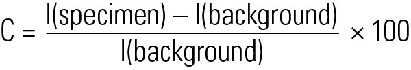
Contrast
The contrast of an image depends on the difference in color and intensity of the depicted object from its background. Expressed in a mathematical formula, contrast (C) can be described as a ratio (in %) of intensities (I) (refer to the equation just below).
Deconvolution
Deconvolution is a technique that reassigns out-of-focus information to its point of origin in a microscope image by applying a mathematical algorithm. By doing so, the user can achieve sharper pictures of specific focus levels and more realistic 3D impressions of the structures of interest.
Dwell time
In confocal microscopy, the laser beam scans an area (the dimension of a pixel of the equivalent image) for a given time. The time to scan this area is called the dwell time. It is possible that extended dwell times lead to photobleaching which can stress the specimen.
Imaging Speed
The imaging speed of a digital camera is measured in frame rates indicated as frames per second (fps). This is the number of images (frames) the camera can acquire in one second. Some sensors are able to read out significantly faster than others, but several other factors can affect the maximum achievable frame rate of a camera. At a given exposure time, the following parameters need to be considered:
- Bit depth;
- Read-out mode (HW vs SW triggering and streaming mode);
- Computer interface (USB2 / USB3 / CamLink, 10GigE, etc.); and
- Computer processing power.
Using a sub-region of a sensor is often a simple way to increase imaging speed.
Related articles
Understanding Clearly the Magnification of Microscopy

What is Empty Magnification and How can Users Avoid it

Introduction to Widefield Microscopy

Depth of Field in Microscope Images
 which was imaged with extended depth of field (EDOF) using digital microscopy.")
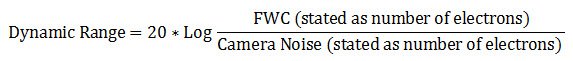
Dynamic range
The dynamic range of a microscope camera gives information on the lowest and highest intensity signals a sensor can record simultaneously. With a low-dynamic-range sensor, bright signals can saturate the sensor, whereas weak signals become lost in the sensor noise. A large dynamic range is especially important for fluorescence imaging. Because the dynamic range is directly connected to the full-well capacity (FWC) [see below], it can be expressed in mathematical terms as the FWC divided by the camera noise:
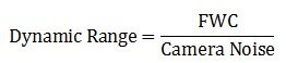
It is can also be described in decibel units (dB):
For fluorescence applications, a large dynamic range is a major benefit to document bright fluorescence signals against a dark background (refer to figure 2) and is especially important when quantifying signals.

The dynamic range is directly affected by the applied gain. Here the term “gain” is used to express the amplification of a generated signal. If gain of a sensor is doubled, then the FWC is effectively cut in half, which in turn decreases the dynamic range. Thus, a trade-off between sensitivity and dynamic range is often required. Many cameras offer different bit-depth modes with different default gain settings optimized for specific applications (speed, sensitivity, and dynamic range). So, in some cases, adjusting the bit setting on the cameras can also impact the dynamic range which may not always be apparent to the user.
If the inherent dynamic range of the sensor is not sufficient for the application or sample or specimen, one may consider a “high-dynamic range” (HDR) acquisition. During this procedure, a series of images is acquired with varying exposure intensities. The resulting image is finally calculated by applying different algorithms (refer to figure 3). The drawback of this approach is the elongated time needed to acquire images. Therefore, it is not preferable for fast moving or light-sensitive samples.
 and a weak fluorescence signal (lower part).")
Exposure time
The exposure time of a digital camera determines the duration the camera sensor is exposed to light from the sample. Depending on the light intensity, exposure times can typically range from milliseconds to a few seconds for most imaging applications.
Full-well capacity (FWC)
The full-well capacity (FWC) is largely dependent on the physical size of the pixel. It refers to the charge storage capacity of a single pixel. This is the maximum number of electrons it can collect before saturation. Reaching the full-well capacity can be compared to a bucket filled with water (refer to figure 4). Larger pixels have a greater FWC than small pixels (typically 45,000 e- for 6.45 µm pixel vs 300,000 e- for a 24 µm pixel). Spatial resolution is sacrificed for the larger FWC which in turn influences the dynamic range (see above). Some modern sensors have optimized pixel designs so relatively small pixels can accommodate a relatively large dynamic range.
 can be compared to a bucked filled with water. Larger buckets can hold more water, like larger pixels can hold more electrons, than smaller ones.")
Any signal exceeding the FWC cannot be quantified. In some instances, the charge can leak into adjacent pixels causing an effect known as blooming (refer to figure 5). Some sensors contain anti-blooming electronics which attempt to bleed off the excess charge to suppress blooming artifacts. Imaging software typically have an overglow tool that enables users to see if any regions of an image are saturated.

Gain
Digital cameras translate photon data into digital data. During this process, electrons coming from the sensor run through a pre-amplifier. Gain is the amplification applied to the signal by the image sensor. It should be noted that not only the signal, but also the noise is increased.
Gamma (Correction)
The human eye’s light perception is non-linear. Our eyes would not perceive two photons to be twice as bright as one; we would only recognize them to be a fraction brighter than one. In contrast to the human eye, a digital camera’s light perception is linear. Two photons would induce twice the amount of signal as one. Gamma can be considered as the link between a human eye and digital camera.
This can be expressed in the following term, where Vout is the output (detected) luminance value and Vin is the input (actual) luminance value:
Vout = Vingamma
By changing gamma – doing gamma correction – it is possible to adapt the digital image taken with a linearly recording camera to the non-linear perception of the human eye. Digital imaging software often has its own gamma correction option.
Intensity
Intensity is an energy classification. In the field of optics the term radiant intensity is used to describe the quantity of light energy emitted by an object per time and area.
Noise
Noise is an undesirable property inherent in all measurements. It is a major concern for scientific images as it can affect the ability to quantify signals of interest. The most important parameter to consider when imaging is the signal-to-noise ratio (SNR) which is the ratio of noise in the image relative to the amount of signal being collected. Noise can be classified into several categories:
Optical noise
Unwanted optical signal often caused by high background staining, resulting poor sample preparation or high sample auto fluorescence. Imaging with a microscope set up in a dark environment will also have a significant impact on optical noise.
Dark noise
Thermal migration of electrons in the sensor and directly proportional to the length of integration. Dark noise can be overcome by cooling the imaging sensor or decreasing exposure time. Also known as dark current, it is a fundamental noise present in the sensor. Dark noise is caused by thermal energy in the silicon randomly generating electrons in pixels. Dark noise builds up in pixels with exposure time. It is expressed in electrons per pixel per second (e-/px/sec). It is less of a concern for fast applications with short exposure times. When it comes to long exposure times, e.g., one second or more for weak fluorescent signals, dark noise can become a major issue. Dark noise is reduced by cooling the sensor, with every 8 °C of cooling halving the dark current (refer to figure 6).

Read noise
An electrical noise source introduced into the signal as the charge is read out from the camera sensor. Read noise can be reduced by slowing the sensor readout rate, thus reducing maximum achievable frame rates. Most modern CMOS sensor are able to read out rapidly (10s of fps), while offering a low read noise. Some high-performance CMOS sensors have a read noise below 1 electron. It originates from the electrical readout circuitry of the sensor involved in quantifying the signal. This pixel readout rate defines how fast charge can be read out from the sensor (units of MHz). Some cameras offer the possibility to alter read-out modes enabling cameras to be optimized for fast read-out mode or slower low-noise modes for low light applications. The unit of read noise is e- and is independent of integration time. Read noise together with the dark noise can be used to decide if a particular camera is suitable for low-light fluorescence applications or not.
Photon shot noise
Noise inherent in any optical signal caused by the stochastic nature of photons hitting the sensor. This is only of concern to very low light applications. Collecting more signal reduces the impact of shot noise in an image. It is another source of noise based on the uncertainty in counting the incoming photons. In other words, it arises from the stochastic nature of photon impacts on the sensor, but is not introduced by the sensor itself. It is best explained by imagining someone trying to catch rain drops in buckets. Even if every bucket is of identical size and shape, they will not all catch exactly the same numbers of drops, hence detection of photons on the chip can be visualized as a Poisson distribution.
Under low light conditions, such as fluorescence imaging when the signal intensity is low, the different noise sources can have a major impact on the quality of the image, as it impacts the signal-to-noise ratio (SNR). Using the right camera for the application is essential for capturing good images. The simplest way to improve the SNR is to collect more signal by integrating for longer times or increasing illumination intensity. These approaches are not always feasible at which point lower noise cameras are required.
Nyquist theorem
Imaging in microscopy implies a sampling process - from a signal to a digital image. The Nyquist Theorem describes an important rule for sampling processes. In principle, the accuracy of reproduction increases with a higher sampling frequency.
The Nyquist Theorem describes that the sampling frequency must be greater than twice the bandwidth of the input signal to recreate the original input from the sampled data. In the case of a digital camera, this manifests principally in the pixel size. For best results, a pixel should always be 3 times smaller than the minimum structure which should be resolved, or in other words, a minimum number of 3 pixels per resolvable unit is preferable.
Pixel
A pixel is the basic light-sensitive unit of a camera’s sensor. This applies to all two-dimensional array sensors including CCD, EMCCD, and CMOS microscope cameras. The number of pixels on a sensor is a frequently quoted unit, i.e., a 5-megapixel (MP) camera has 5,000,000 pixels. The number of pixels is often confused with the resolution of the sensor as individual pixels can vary significantly in size on different sensor types. The main element of a pixel in turn is the photosensitive photodiode with silicon coupled to an electron storage well (refer to figure 7). Silicon is responsible for generating the electrons which then can be collected, moved, and finally converted into a digital signal.

Photons hitting the photodiodes (pixels) are converted into electrons. For the case of CMOS sensors (refer to figure 8 and see below), these electrons are read out to a pixel amplifier. The column amplifier reads the accumulated voltage signal from the pixels in the column and the adjacent analog-digital (AD) converter does the digitization and produces equivalent digital signals.

The charge generated in a pixel is directly proportional to the number of photons striking the sensor, which is typically influenced by the duration of light exposure (integration time), the detected wavelength and, most importantly, the light intensity. As a rule of thumb, the pixel size defines the number of electrons which can be collected without saturating a pixel. The size of pixels typically varies between 1 and 16 µm² for microscopy imaging sensors.
Due to typical pixel architectures, the entire surface of a pixel is not photo sensitive. The fill factor of an image sensor describes the relation of a pixel’s light-sensitive area to its overall area. Microlenses can be added to a pixel to better focus the light onto the photosensitive regions improving the fill factor.
A complete digital imaging sensor consists of millions of pixels organized in a geometrical array. Very often the number of pixels is mixed up with “resolution”. It is noteworthy that it is not simply the number of pixels, but their size which is defining the resolution of the camera chip. In general, smaller pixels will give a higher resolution than large ones. In the end, the resolution of a microscopy system depends not only on the sensor array, but the complete optical system with the numerical aperture (NA) of the primary objective being the main factor determining resolution.
Quantum efficiency (QE)
The quantum efficiency (QE) of a sensor indicates how sensitive it is. More precisely, the QE describes the percentage of photons striking the sensor for a given wavelength that will be converted into electrons. The QE curve of a sensor shows how this varies at specific wavelengths.
In an ideal world one would assume that 100 photons are able to generate 100 electrons. When interacting with a sensor, photons may be absorbed, reflected, or even pass straight through. The ability of a sensor to absorb and convert light of a certain wavelength into electrons is the QE.
The QE of a sensor is affected by a number of factors including:
- Fill factor
- Addition / performance of micro lenses
- Anti-reflective coatings
- Sensor format (back or front illuminated)
The QE is always a function of the wavelength of the incoming light. Silicon detectors most commonly used for scientific imaging are able to detect wavelengths just beyond the range of visible light (~400 to 1000 nm). By looking at a QE curve, it’s possible to see how efficient a particular sensor is at converting a particular wavelength into a signal (refer to figure 9).
")
The majority of camera sensors are front-illuminated where incident light enters from the front of the pixel, having to pass semi-opaque layers containing the pixels circuitry, before hitting the photo-sensitive silicon. These layers cause some light loss, so front-illuminated sensors typically have maximum QE’s around 70% to 80%. As the electronics on the surface of sensors are only able to generate a localized electrical field, they’re not able to manipulate the charge that forms deeper in the silicon wafer (refer to figure 10).
In the case of a back-illuminated sensor, light directly hits the photo-sensitive silicon from the “back” without having to pass through the pixel circuitry, offering a maximum QE value approaching 95%. To manufacture back illuminated sensors, also known as back thinned, this additional silicon is ground away to create an incredibly thin silicon layer where all of the charge can be manipulated by the pixels’ electronics.

RGB/Grayscale histogram
Each pixel of an image has a certain grayscale value. The spectrum of grayscale values ranges from pure black (0) to pure white (255 at 8-bit color depth, 4095 at 12-bit color depth, etc.).
Histograms show the distribution of grayscale values within a region of interest (ROI), i.e., the number of pixels is determined for each grayscale value and the result is shown as a curve.
With the help of a histogram (refer to figure 11), settings, such as camera exposure, gain and excitation intensity, can be optimized.

Line profile
This tool measures grayscale values along linear regions of interest (ROIs), displays them graphically as a curve (refer to figure 12), and carries out statistical processing on them.

Stack profile
This tool measures mean grayscale values using regions of interest (ROIs), displays them graphically as a curve (refer to figure 13), and carries out statistical processing on them.

Saturation
The basic working principle of a digital camera implies that photons hitting the photodiodes induce electrons which are collected, moved, and finally converted into a digital signal.
If either is exceeded, the additional information cannot be handled by the camera leading to artifacts in the digital image, e.g., blooming.
N.B.: The Look-up table Glow (O&U) in the LAS X software can help control saturation.
Sensor types for microscope cameras (CCD, EMCCD, CMOS, sCMOS)
Most of the features and parameters described above are generic for all types of imaging sensors in digital microscope cameras. However, based on historical developments and technical improvements, users can select between different types of camera sensors. They differ in the principal architecture (e.g., CCD vs. CMOS) and ability to enhance signals (e.g., EMCCDs vs. CCDs).
CCD Microscope Camera
Microscope cameras based on a Charged Coupled Device (CCD) (refer to figure 14) are less common these day with CMOS technology having largely replaced CCDs. As with any other digital camera sensor, its single pixels generate a charge upon irradiation with light which is finally transformed into a digital signal. With a CCD, the charge generated in the pixels is moved over from one pixel to the other across the surface into the serial register. From the serial register, charges are passed one by one to the read-out electronics where the signal is converted into a voltage, amplified, , and digitized. This architecture means that the data captured by a CCD sensor is read out through a single output node, in contrast to CMOS sensors, enabling excellent image uniformity.
EMCCD Microscope Camera
In simple terms, an EMCCD (Electron Multiplying Charged Coupled Device) sensor is a CCD sensor with the addition of a special EM gain register which is placed between the sensor and the readout electronics (refer to figure 14). This register amplifies the signal. Moreover, EMCCD sensors can be back-thinned and achieve a typical peak quantum efficiency (QE) of more than 90%. These types of cameras are used for extreme low-light applications and can be single photon sensitive. They can cost significantly more than regular CCD cameras.
CMOS Microscope Camera
Complementary Metal Oxide Semiconductor (CMOS) sensors (refer to figure 14) were originally used in cell phones and low-end cameras due to poor image uniformity. In recent years, CMOS-sensor image quality has improved enormously to the point that they are used in almost all scientific and commercial cameras In contrast to CCDs, CMOS sensors handle the change-to-voltage conversion in each pixel. The read-out and digitization process is massively parallelized with read-out nodes at the end of each column. Unlike traditional CCD sensors which use only a single read-out node, this architecture enables CMOS sensors to read out high pixel-count arrays much faster without increasing read noise.

Signal-to-noise ratio
The signal-to-noise ratio (SNR) measures the overall quality of an image. The higher the SNR, the better the image (refer to figure 15). Signal refers to the number of photons originating from the region of interest (ROI) of a sample or specimen collected by the sensor and converted into an electrical signal. Noise refers to the unwanted signals introduced into the image by the detector itself or originating from background optical signals.

SNR is heavily influenced by the sensor type. Broadly speaking it can be designated as a sensor’s sensitivity. Although this can be complex, the SNR expresses how well a signal of interest is distinguished from the background noise (refer to figure 16). There are several factors to explore here, as the signal depends on the number of photons arriving at the sensor, the sensor’s ability to convert those photons into a signal, and how well the camera can suppress unwanted noise. Finally, it is important to mention that optical noise from the sample, auto fluorescence, or poor staining is often the dominant noise source of an image. The use of advanced sensors cannot help users overcome a poorly prepared sample.
")
Summary
Modern optical microscopy is unimaginable without the use of digital cameras. Most microscope users either want to watch their sample or specimen live on a monitor or save and analyze their data to extract more complex information. Moreover, many modern microscopic techniques would not have been even possible without the advancement of digital camera sensors. This article gives an overview of how digital microscope images are produced. It is intended to help users learn how to use a digital camera in the right way and interpret the generated data correctly.
References
- L. Felts, V. Kohli, J.M. Marr, J. Schumacher, O. Schlicker, An Introduction to Computational Clearing: A new method to remove out-of-focus blur, Science Lab (2020) Leica Microsystems.
- J. Schumacher, L. Bertrand, Real Time Images of 3D Specimens with Sharp Contrast Free of Haze: Technology Note THUNDER Imagers: How do they really work?, Science Lab (2019) Leica Microsystems.
- E. Darling, Computational Clearing - Enhance 3D Specimen Imaging: Free Webinar On-Demand, Science Lab (2020) Leica Microsystems.
 2D slices of a 1 mm diameter midbrain neural organoid stained with DAPI (blue, nuclear stain), β-tubulin (green, neuronal stain), and GFAP (red, astrocyte stain).")


