EM TXP
전자현미경 시료 전처리
제품소개
홈
Leica Microsystems
EM TXP 단면 절단 장치
최신 기사를 읽어 보세요
Workflow Solutions for Sample Preparation Methods for Material Science
This brochure presents and explains appropriate workflow solutions for the most frequently required sample preparation methods for material science samples.

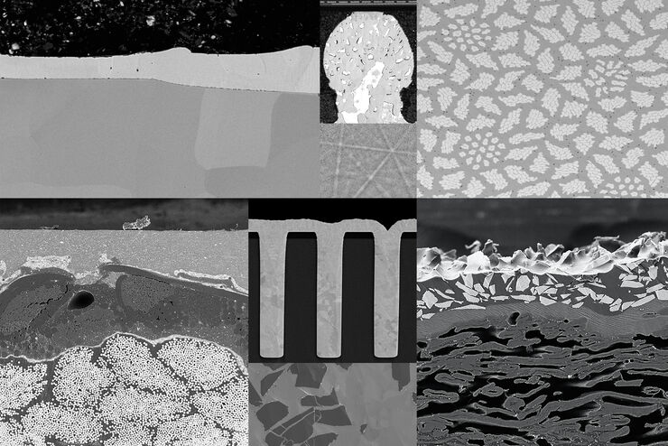
Quality Control via Cross Sections of PCBs, PCBAs, ICs, and Batteries
Why cross sections of printed circuit boards (PCBs) and assemblies (PCBAs), integrated circuits (ICs), and battery components are useful for quality control (QC), failure analysis (FA), and research…
 chip cross section acquired at higher magnification showing a region of interest.")
Structural and Chemical Analysis of IC-Chip Cross Sections
This article shows how electronic IC-chip cross sections can be efficiently and reliably prepared and then analyzed, both visually and chemically at the microscale, with the EM TXP and DM6 M LIBS…
. The grains are highlighted with arbitrary colors.")
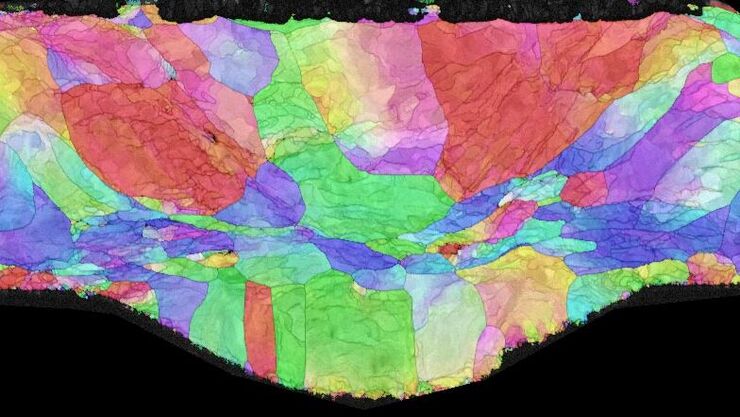
High-Quality EBSD Sample Preparation
This article describes a method for EBSD sample preparation of challenging materials. The high-quality samples required for electron backscatter diffraction are prepared with broad ion-beam milling.

How to Prepare and Analyse Battery Samples with Electron Microscopy
This workshop covers the sample preparation process for lithium and novel battery sample analysis, as well as other semiconductor samples requiring high-resolution cross-section imaging.

Cross Section Ion Beam Milling of Battery Components
Sample Preparation of Lithium battery systems requires high quality surface preparation to evaluate their internal structure and morphology. Due to the brittle materials involved, preparing pristine…
Ion Beam Milling Guide: Enhancing Surface Quality for High-Resolution Imaging and Analysis
In this article you can learn how to optimize the preparation quality of your samples by using the ion beam etching method with the EM TIC 3X ion beam milling machine. A short introduction of the…
재료 과학 & 분석
재료 과학 & 분석에서 현미경은 중요한 역할을 합니다. 연구 및 품질 관리를 위해 금속 합금, 세라믹, 폴리머를 분석하는 데 사용됩니다.
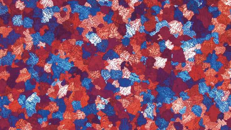
금속학
금속, 합금, 기타 재료의 미세 구조 분석은 라이카 금속 현미경 솔루션을 활용하여 최적화할 수 있습니다.
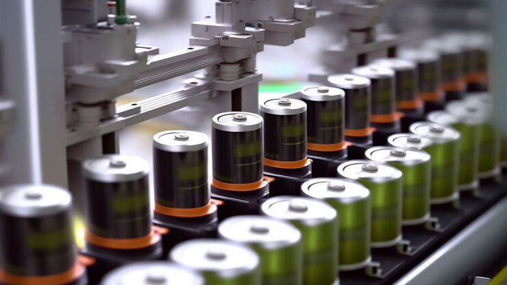
배터리 제조
배터리 제조에는 검사와 관련된 몇 가지 주요 과제가 있습니다. 여기에는 샘플 준비, 현미경 육안 검사 및 화학 분석을 위한 솔루션이 필요합니다.
Fields of Application
시계 제조업
시계 제조업자와 시계 제조 산업에 있어서, Leica 실체 현미경의 높은 정밀도는 정교하게 이뤄지는 시계 조립과 높은 품질과 기술력을 보증하기 위한 신뢰할 수 있는 검사 과정을 용이하게 합니다. 저희의 인체공학적 액세서리를 사용하면, 현미경으로 장시간을 작업해도 피로를 줄일 수 있도록 고객의 필요에 따라 기기를 최적으로 구성할 수 있습니다.
자동차 분야
Leica는 최적의 이미징 솔루션을 제공하는 신뢰할 수 있는 파트너가 되어 고객이 경쟁에서 앞서 나갈 수 있기를 희망합니다.
산업용 현미경 시장
가동 시간을 최대화하고 목표를 달성하면 수익에 효율적으로 도움이 됩니다. Leica 현미경 솔루션은 가장 작은 샘플 세부 사항에 대한 통찰력을 제공할 뿐만 아니라 결과를 빠르고 안정적으로 분석, 문서화 및 보고할 수 있습니다. Leica Microsystems는 다양한 애플리케이션 요구 사항을 충족하는 데 도움이 되는 광범위한 솔루션과 전문가 지원을…
전자 장치의 단면 분석
전자 장치의 단면 분석을 통해 인쇄 회로 기판(PCB), 조립품(PCBA) 및 집적 회로(IC)와 같은 부품의 고장 메커니즘을 상세히 분석할 수 있습니다.
전자 및 반도체 산업
전자 및 반도체의 경우 효율적인 검사, 단면 및 청정도 분석, PCB, 웨이퍼, IC 칩 및 배터리의 R&D를 지원하는 솔루션이 중요합니다.
배터리 제조
배터리 제조에는 검사와 관련된 몇 가지 주요 과제가 있습니다. 여기에는 샘플 준비, 현미경 육안 검사 및 화학 분석을 위한 솔루션이 필요합니다.
재료 과학 & 분석
재료 과학 & 분석에서 현미경은 중요한 역할을 합니다. 연구 및 품질 관리를 위해 금속 합금, 세라믹, 폴리머를 분석하는 데 사용됩니다.
