 and oblique (right) brightfield illumination using a Leica compound microscope. The defect on the wafer surface is clearly more visible with oblique illumination.")
How semiconductor manufacturing benefits from microscopy
Microscope solutions serve an important role for efficient and reliable inspection, quality control (QC), failure analysis (FA), and research and development (R&D) in the semiconductor manufacturing industry.
During the manufacturing of semiconductors, many types of defects can occur during different steps which can be detrimental to the proper functioning of the device. The earlier such defects are detected the better. These defects may be due to dust particles randomly distributed on the wafer (random defects), or scratches, detachments, and residues of coatings and photoresists due to processing conditions, e.g. during patterning, and will occur on specific regions of the wafer. Due to their small size, microscopy is a tool of choice for identifying such defects.
In particular, optical microscopy (OM) offers many advantages over slower and more expensive alternatives like electron microscopy (EM). Due to its versatility and ease of use, OM is often used to both qualitatively and quantitatively investigate defects on both bare and patterned/processed wafers, but also during assembly and packaging of ICs (integrated circuits).
Different OM contrast methods, such as brightfield (BF), darkfield (DF), differential interference contrast (DIC), polarization (POL), UV (ultraviolet), oblique illumination, and infrared (IR) transmitted light [1-4] can be crucial for rapid, accurate detection of defects during wafer and IC-chip inspection.
Challenges to Overcome during Inspection
There is an ever-increasing demand for the use of larger wafers in production, along with a rapidly decreasing size of patterned structures and microelectronic components. The ever-smaller size makes it challenging at times to visualize surface structures and defects on semiconductor materials, processed wafers, and IC chips with optical microscopy. For efficiency when inspecting, users need to scan quickly large areas of a wafer or material at low magnification to identify areas of interest (refer to figure 1) and then observe accurately very fine details, structures, and defects at higher magnification.
Some defects, e.g. dust, scratches, detachments, or residues of coatings and photoresists, on processed wafers, may be difficult to see with conventional optical microscopy. In this case, there would be a need to transfer the samples to an electron microscope or other instrument. However, examples of how different optical-microscope contrast methods can make semiconductor and wafer inspection efficient are shown below.
 and a large field of view with the goal of finding an area of interest during inspection.")
Microscope contrast methods
Basic background information on the OM contrast methods BF (brightfield), DF (darkfield), DIC (differential interference contrast), POL (polarization), UV (ultraviolet), oblique illumination, and IR TL (infrared transmitted light) [1-4] for imaging of opaque materials (visible spectrum), like semiconductors, with incident light is given below. More details about these contrast methods can be found in references 1 to 4.
When using the common BF illumination, it can be challenging to see some wafer defects. So other contrast methods, DF, DIC, POL, UV, and oblique illumination [1-4], may be required to see them clearly, making the transfer of samples to an electron microscope or other instrument unnecessary.
BF illumination [1-3] is the most common method used to detect defects. During BF imaging, the incident white light directly reflected from the surface of the semiconductor or wafer sample is observed. Flat and shiny surfaces reflect a large amount of light back towards the eyepieces or camera, so the sample appears bright when observed. In comparison, patterned surfaces with holes and other features scatter the light, so the sample appears darker, producing more contrast. However, for reflective samples some structures can still be “drowned out” by the bright illumination, so not easily visible. Examples of wafer images taken with BF illumination are shown in figure 2.
 taken with BF illumination to search for defects, particles, and contamination")
DF illumination is also relatively common [1-3]. During DF imaging, the majority of the incident white light does not reflect back towards the objective, but actually misses it, as the light impinges on the sample surface at a high angle with respect to the vertical direction. So there is no risk that bright light “drowns out” sample structures. Only some light which is scattered from non-flat surface features can actually reach the eyepieces or camera. Flat areas of the surface appear dark, while non-flat patterned areas, where there are even very small features like pores, bumps, scratches, and dust particles, appear brighter. Examples of wafer images taken with DF illumination are shown in figure 3.
 acquired with DF illumination (compare with figures 2 and 4-5): A) center of the whole square in figure 1 and B) IC-patterned wafer.")
Both BF and DF can be used to acquire information concerning lateral dimensions, but little or no information about the vertical dimension.
DIC imaging is less often used than either BF or DF [1-3]. It uses a prism which separates polarized incident white light into 2 light beams which reflect from the sample surface and then repass through the prism and merge back together. The remerged beams interfere, forming elliptically polarized light, and then passes through an analyzer. This interference makes it possible to visualize small height variations of patterns and structures on the sample surface. Examples of wafer images taken with DIC illumination are shown in figure 4.
 taken with DIC illumination (compare with figures 2-3 and 5): A) center of the whole square in figure 1 and B) IC-patterned wafer.")
POL imaging is less often used than either BF, DF, or DIC [1-4]. POL imaging uses 2 polarizers to provide information about optically anisotropic materials. Contrast comes from the interaction of plane-polarized light with a birefringent, i.e., double refracting, sample, creating out-of-phase light waves. These waves are then recombined by the second polarizer (also called analyzer) to provide information about the structure and composition of the sample.
UV imaging is not as common as the other contrast methods above, but it offers significant advantages [2]. It exploits the shorter wavelength of incident ultraviolet light, enabling higher resolution than visible light [2,5], and reveals finer details, structures, and defects on the wafer or semiconductor surface. These small structures and defects would not always be clearly visible with BF, DF, DIC, or POL imaging using white light. With visible white light (400-700 nm) illumination the lateral resolution is limited to 0.25 µm and with UV light (365 nm) illumination it is limited to 0.12 µm [2]. Examples of wafer images taken with UV illumination are shown in figure 5.
 acquired with UV illumination (compare with figures 2-4): A) a flip-chip montage with bumps and B) a processed wafer.")
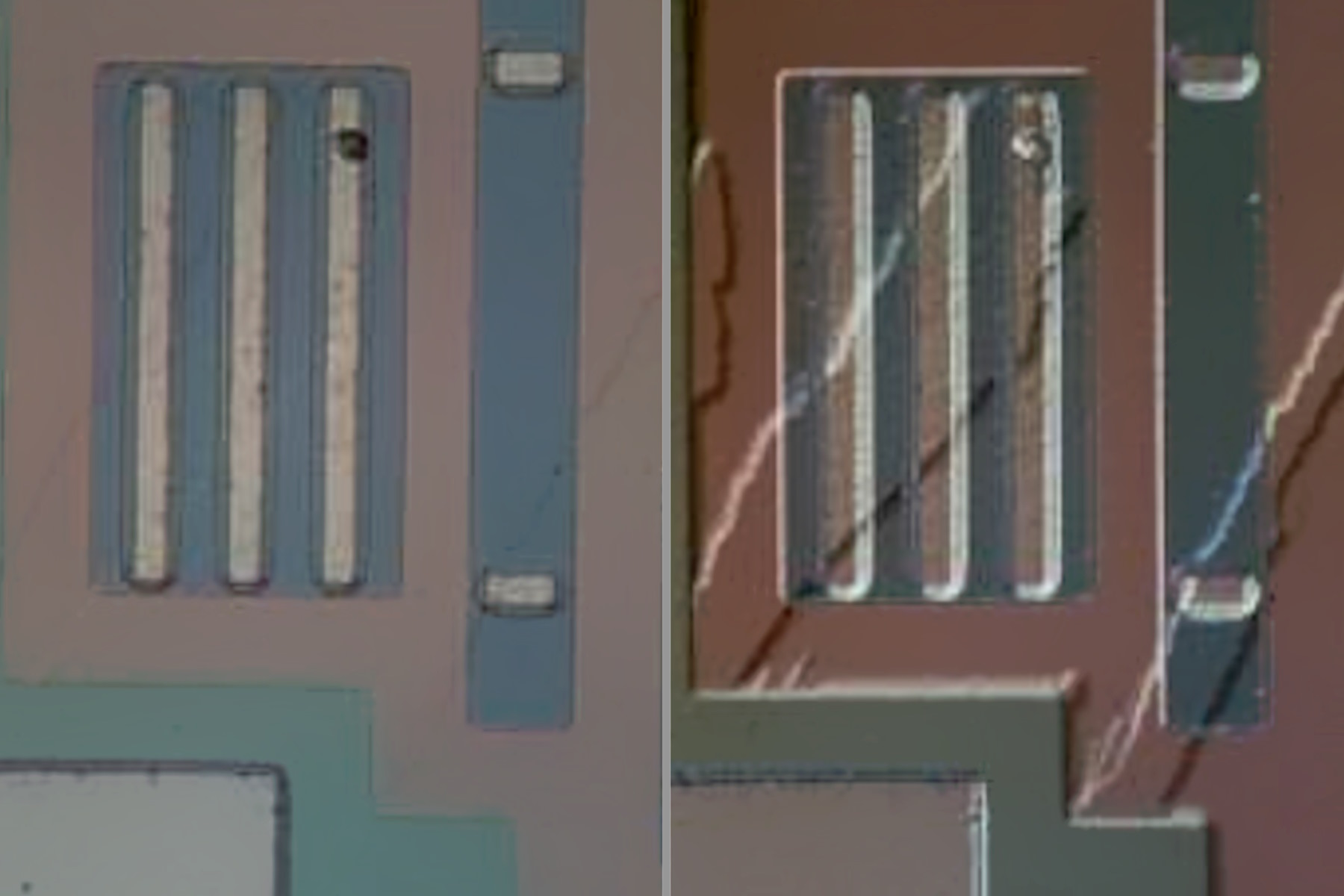
Oblique illumination is simply the use of incident visible (BF) or UV light where it impinges the sample surface at an oblique angle [2]. It reveals structures and defects on the wafer or semiconductor surface better, as it gives them more contrast than normal incident illumination alone [2]. Examples of wafer images taken with oblique BF and UV illumination are shown in figure 6.
 and BF (OBF) illumination")
Semiconducting materials like Si are usually transparent to infrared (IR) light (wavelengths of 1000 nm or greater). This fact means IR illumination can be exploited to visualize details below a wafer’s surface which are otherwise hidden when observed with visible light. Therefore, IR illumination makes it possible to see defects associated with a sub-surface embedded layer. An example of a wafer image taken with IR illumination is shown in figure 7.
 taken with A) IR and B) BF illumination. In the IR image sub-surface structures can be seen.")
Microscope solutions can help overcome inspection challenges
Rapid and reliable semiconductor, wafer, and microelectronics inspection can be achieved with a microscope solution offering many if not all of the above contrast methods. The images shown in figures 2 to 5 above demonstrate how a change of contrast method and illumination can make a difference. The advantage is especially noticeable when comparing BF to UV or oblique illumination (refer to figures 2B to 2D and 5A to 5F).
There are Leica microscope solutions which can help users achieve this goal: the DM8000 M and DM12000 M. They offer all the BF, DF, DIC, POL, UV, and oblique contrast methods and enable users to perform efficient active screening and detection of macroscopic to microscopic defects on the sample surface with the macro to micro inspection mode. This mode enables an easy change of objectives over a range of magnification values from 0.7x up to 150x (refer to figures 1, 2A, 3A, and 4A).
Summary / conclusions
Efficient and accurate inspection to detect defects, structures, and contamination on semiconductor materials, processed/patterned wafers, and IC chips can be achieved by using an optical microscope solution which provides contrast methods using brightfield (BF), darkfield (DF), differential interference contrast (DIC), polarization (POL), UV (ultraviolet), oblique, and infrared (IR) illumination. A fast scan overview of the sample at low magnification and resolution is first done to identify areas of interest. Next, the detection and observation of fine details, small structures, defects, and contamination on the sample surface is performed at high magnification and resolution. Users can take advantage of Leica microscopes offering these contrast methods.
References
- D. Dionis, J. DeRose, Section “Beyond brightfield” in Metallography - an Introduction: How to Reveal Microstructural Features of Metals and Alloys, Science Lab (2020) Leica Microsystems.
- M. Doppler, How to Boost your Microelectronic Component Inspection Performance: Overcoming the resolution criterion - Webinar on-demand, Science Lab (2021) Leica Microsystems.
- D. Dionis, J. DeRose, Section "Incident illumination contrast methods" in How to Adapt Grain Size Analysis of Metallic Alloys to Your Needs: Precise and practical microscopy solutions, Science Lab (2019) Leica Microsystems.
- W. Ockenga, Polarization Contrast: An introduction, Science Lab (2011) Leica Microsystems.
- M. Wilson, J. DeRose, C. Greb, Microscope Resolution: Concepts, Factors and Calculation: Airy discs, Abbe’s diffraction limit, the Rayleigh Criterion, and the point spread function (PSF), Science Lab (2023) Leica Microsystems.
Related Articles
-
 chip cross section acquired at higher magnification showing a region of interest.")
Structural and Chemical Analysis of IC-Chip Cross Sections
This article shows how electronic IC-chip cross sections can be efficiently and reliably prepared…
Sep 05, 2023Read article -
Rapid and Reliable Examination of PCBs & PCBAs with Digital Microscopy
Digital microscopes provide users with a convenient and rapid way to acquire high-quality, reliable…
Jul 06, 2023Read article -

How to Boost your Microelectronic Component Inspection Performance
Do you need to see more when inspecting silicon wafers or MEMS? Would you like to get sharp and…
Nov 24, 2021Read article