Cross-Section Analysis for Electronics
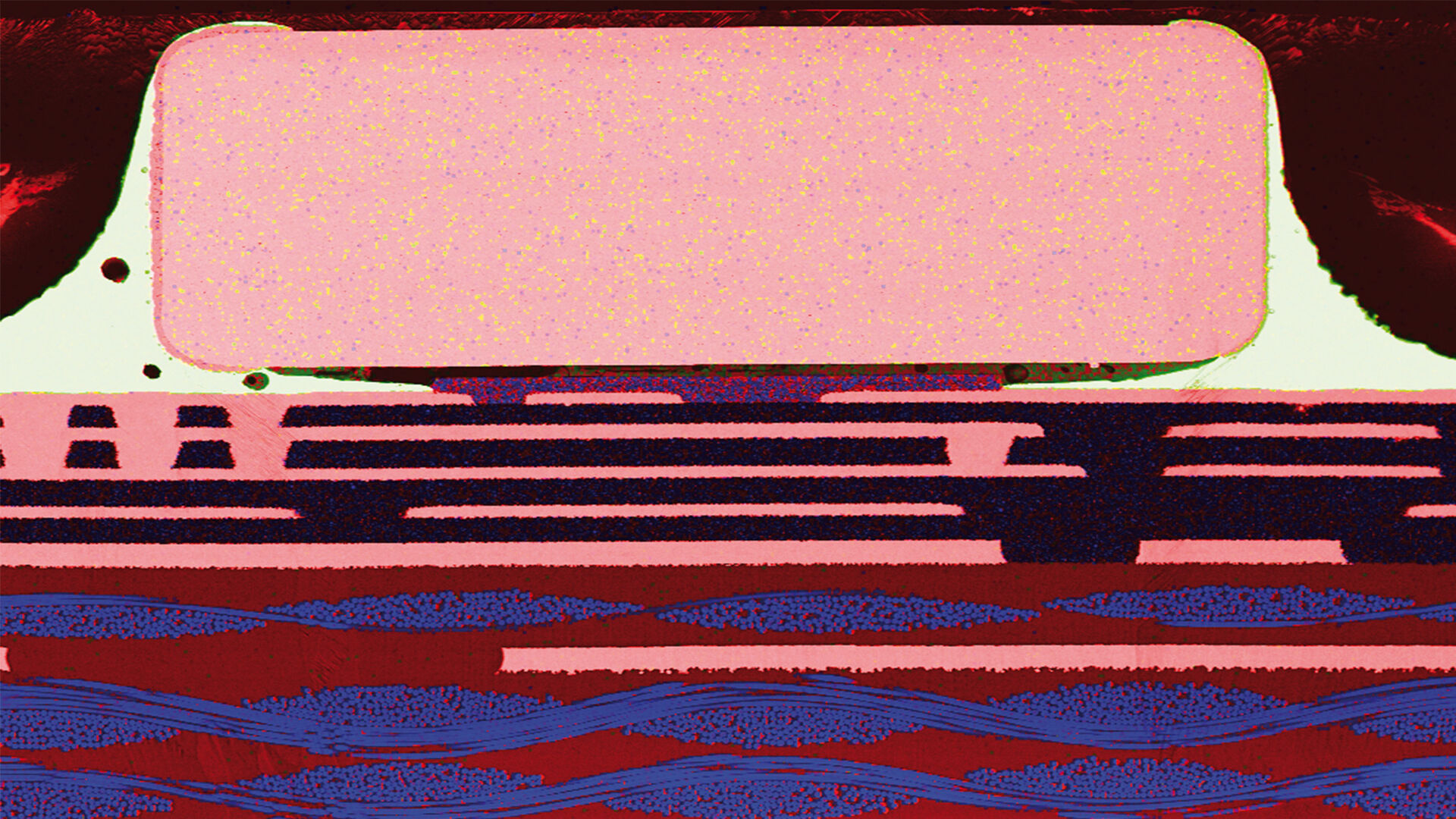
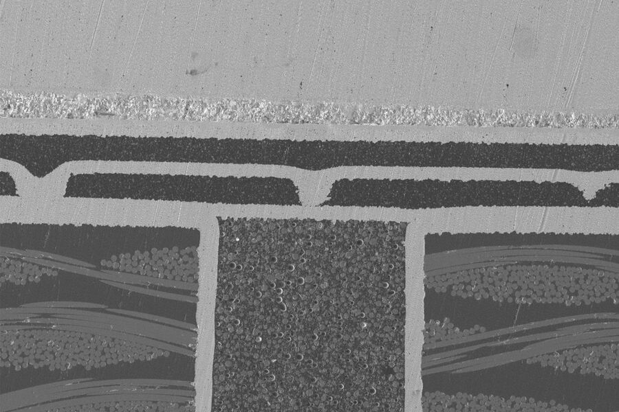
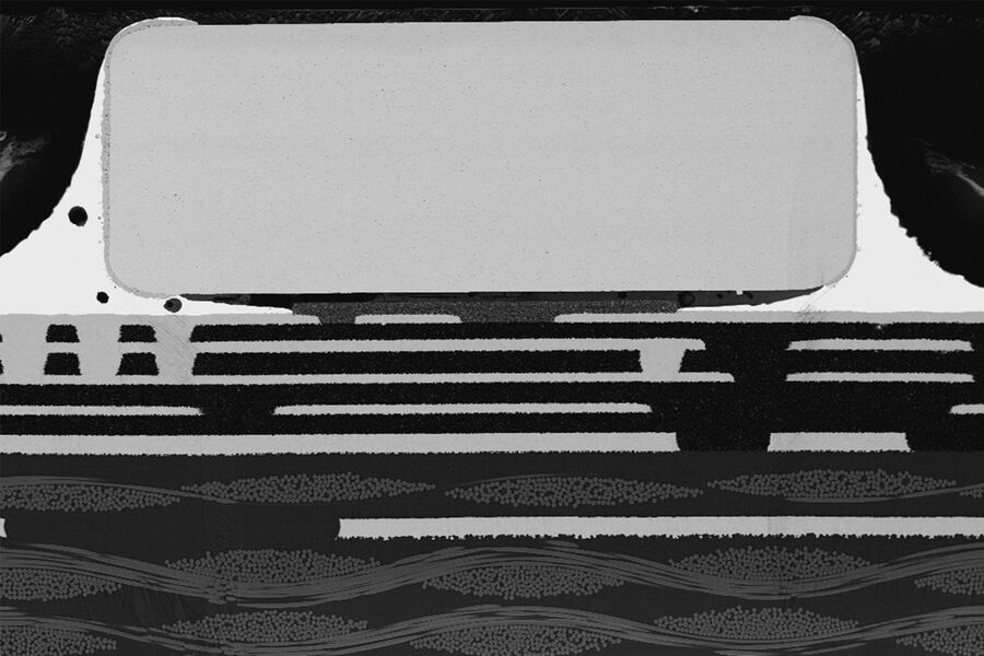
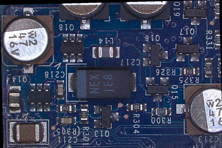
Cross-section analysis for electronics is used to examine the internal microstructure of electronic components like printed circuit boards (PCBs), assemblies (PCBAs), and integrated circuits (ICs). These components are often made from opaque, non-transparent materials. For cross-section analysis, a cross section of the component is made and analyzed with optical and electron microscopy and spectroscopy to reveal the structure and composition of grains, phases, layers, interfaces, cracks, voids, defects, etc. Cross-section analysis is useful for quality control (QC), failure analysis (FA), and research and development (R&D) of PCBs, PCBAs, ICs, and other electronic components.
Contact a local imaging specialist for expert advice on cross-section analysis for your needs and budget.

What is a cross section in manufacturing?
For cross sectioning of materials like metal alloys, ceramics, printed circuit boards (PCBs) or assemblies (PCBAs), or integrated circuits (ICs), a slice is made across its volume in a specific orientation to expose the bulk. The internal microstructure can then be observed. For PCBs and ICs, cross sectioning is useful for quality control and failure analysis.

What is a cross section of a material or product?
A cross section is a slice of a material or product, e.g., a metal, ceramic, polymer, composite material, mineral, circuit board, or integrated circuit, which allows the internal structure to be examined. A sample of the material or product is cut along a specific axis of orientation, ground, and then polished to create a smooth, flat surface. Analysis is often done with optical or electron microscopy or spectroscopy.

What is the purpose of cross sectioning?
Cross sectioning is very useful for quality control and failure analysis. It is used to evaluate the structural integrity of electronic components, like printed circuit boards (PCBs) and assemblies (PCBAs), integrated circuits (ICs), substrate materials and layers, interconnections, wire bonds, solder joints, and encapsulation materials. Cross-section analysis helps identify defects which can cause component failure.
Get your individual solution based on 3 short questions.
Dedicated configurations are available for your specific needs. Answer the short questionnaire to find the right solution for your needs. If you would rather have a representative contact you, then please click here to fill out your contact information.
Contact us{{ question.questionText }}
Please select an answer!
Best Match
{{ resultProduct.header }}
{{ resultProduct.subheader }}
{{ resultProduct.description }}
{{ resultProduct.features }}
Request Your Information Package
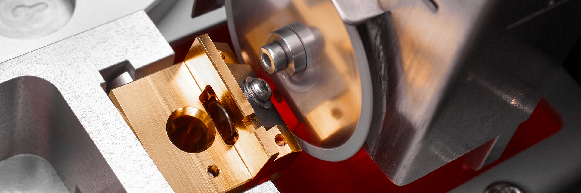
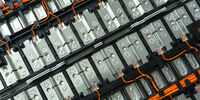
Preparation of PCB/PCBA cross section
The preparation of a PCB/PCBA cross section involves multiple steps:
- Cutting out a slice of the printed circuit board (PCB) or assembly (PCBA) from a selected area.
- Cleaning, mounting, grinding, polishing, ion milling, and sometimes etching the cross section to reveal the internal microstructure and different layers of the PCB/PCBA.
The result is a smooth and flat surface that can be observed easily with optical (OM) or electron microscopy (EM). Examination with OM or EM enables assessment of the microstructure and various layers.
Preparation of IC cross section
Preparing a cross section of an integrated circuit (IC) can typically require:
- Selecting and cutting out a specific area to be analyzed
- Removal of the encapsulation materials
- Embedding the IC sample in an epoxy resin
- Cutting out a thin slice with sawing or ion beam milling to expose the IC internal structure
- Grinding and polishing to obtain a smooth surface
- Selective etching may be used to reveal specific IC structures
- Visualizing and analyzing the IC cross section with optical and electron microscopy and spectroscopy, e.g., compound microscope with LIBS or SEM with EDS, to reveal the fine details and internal microstructure.
Related Articles Cross-Section Analysis for Electronics
 at the edge of a battery electrode acquired with a DVM6 digital microscope.")
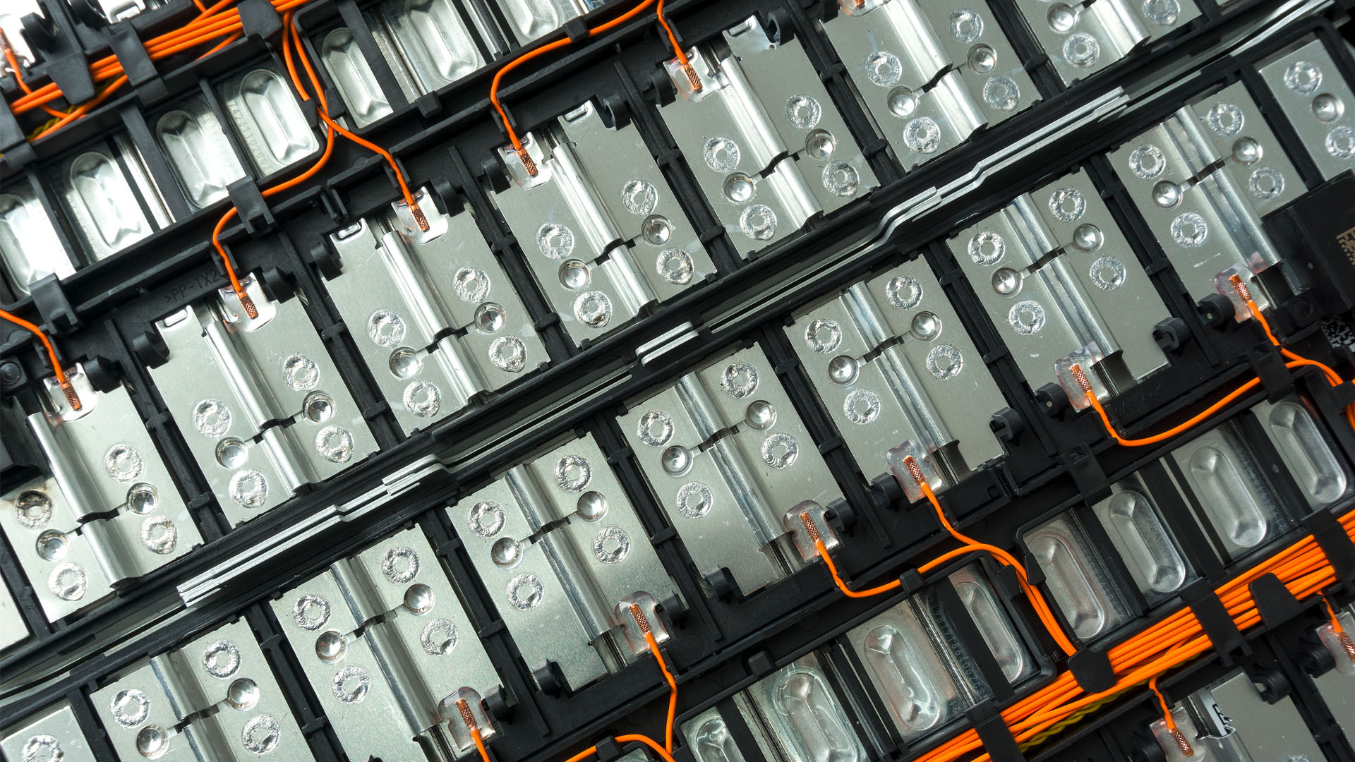
Burr Detection During Battery Manufacturing

Battery Particle Detection During the Production Process

Key Factors for Efficient Cleanliness Analysis
 and oblique (right) brightfield illumination using a Leica compound microscope. The defect on the wafer surface is clearly more visible with oblique illumination.")
Rapid Semiconductor Inspection with Microscope Contrast Methods

Cross-section Analysis for Electronics Manufacturing
 chip cross section acquired at higher magnification showing a region of interest.")
Structural and Chemical Analysis of IC-Chip Cross Sections
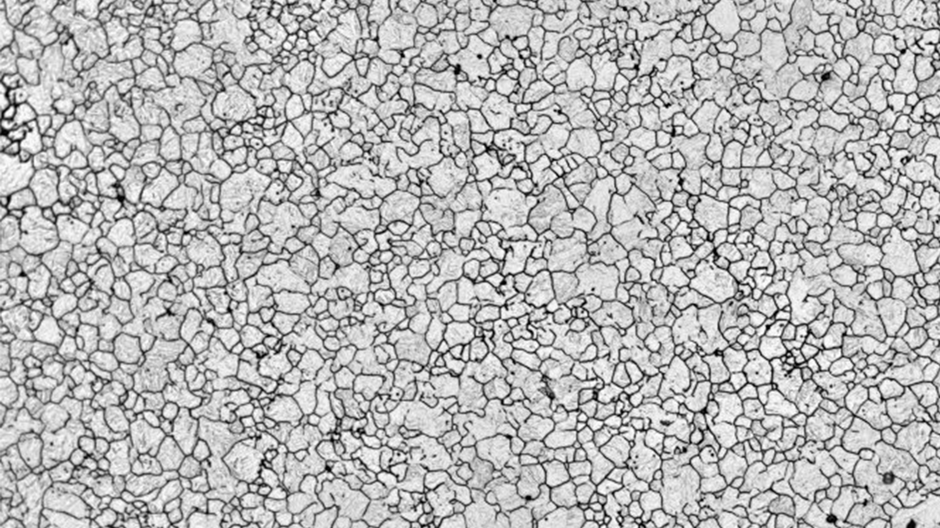
. The grains are highlighted with arbitrary colors.")
High-Quality EBSD Sample Preparation

Key Factors to Consider When Selecting a Stereo Microscope
Rapid and Reliable Examination of PCBs & PCBAs with Digital Microscopy

What is the FusionOptics Technology?


Interested to know more?
Talk to our experts.
Do you prefer personal consulting? Show local contacts