재료 과학 & 분석

재료 과학 & 분석 현미경은 금속 합금, 반도체, 유리, 세라믹 및 플라스틱과 같은 재료 분석에 사용됩니다. 라이카 마이크로시스템즈는 품질 관리, 고장 분석, R&D를 지원하는 고급 현미경 솔루션을 제공하여 보다 심층적인 통찰력을 얻을 수 있도록 지원합니다.

지원 문의하기

재료 과학 & 분석을 위한 현미경 분석 솔루션에 대한 개인적인 전문가 조언이 필요하시면 저희에게 문의하시기 바랍니다.

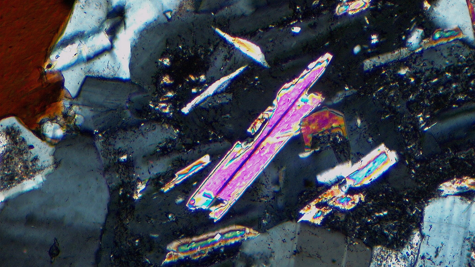
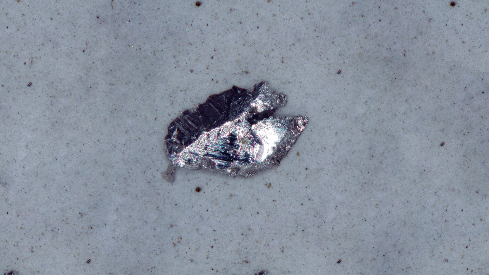
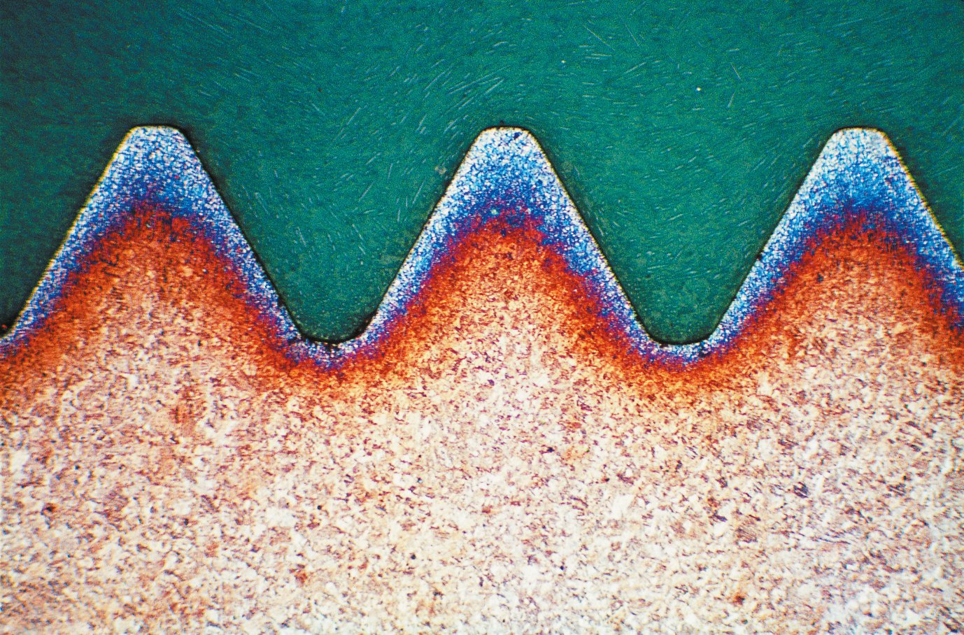
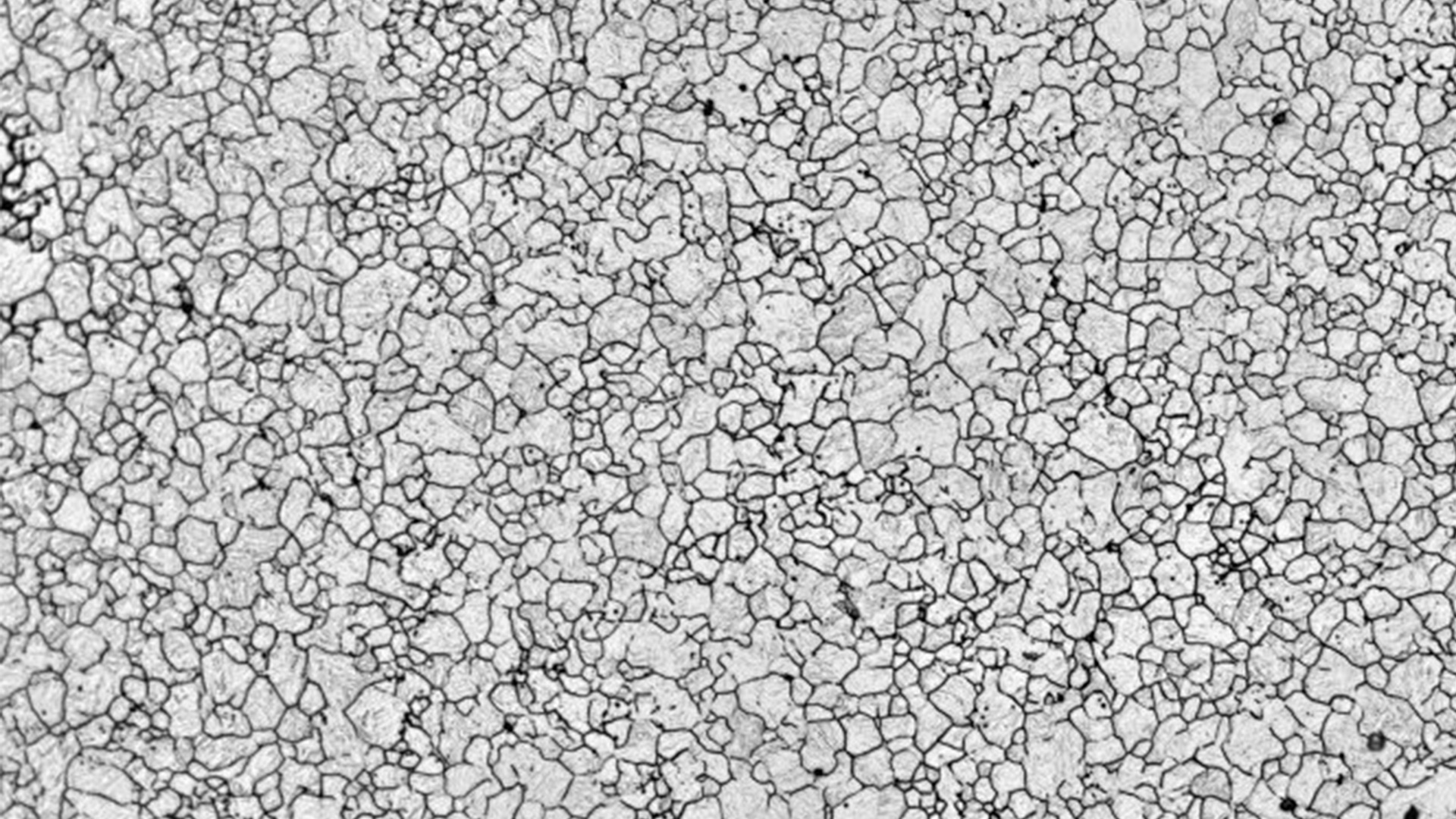
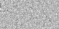
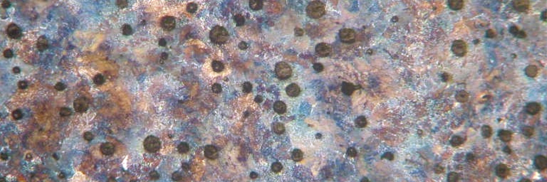
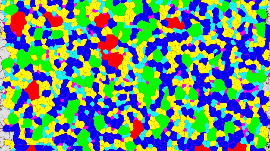
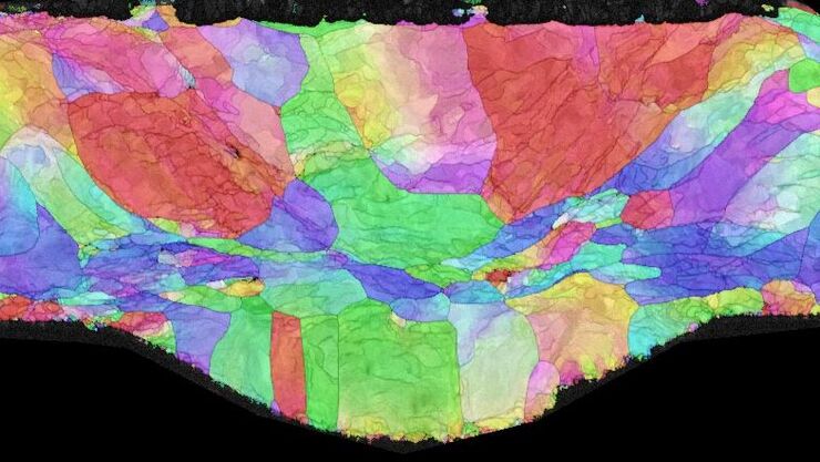
불순물과 내부 구조는 어떻게 분석하나요?

편광 및 차등 간섭 대비(DIC)가 적용된 현미경을 사용하면 표준 명시야 조명으로는 보이지 않는 미세 균열이나 내포물과 같은 내부 재료 구조를 시각화할 수 있습니다. 편광은 이방성 물질을 강조하고 DIC는 염색 없이 투명한 시료의 대비를 향상시킵니다. DM4 P 및 DM6 M 현미경은 편광 및 DIC를 제공합니다.

현미경 이미징 샘플을 정밀하게 준비하는 방법은 무엇인가요?

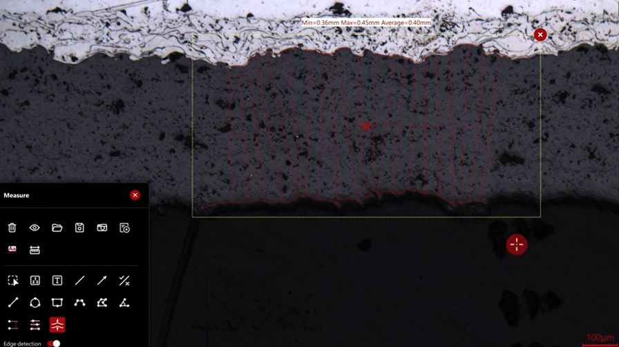
단단한 재료를 정밀하게 절단, 연마, 연마하여 특정 샘플 영역을 미크론 단위의 정밀도로 타겟팅할 수 있습니다. EM TXP 타겟 준비 시스템을 사용할 때 가능합니다.

이질적이거나 부서지기 쉬운 재료와 매우 평평한 표면의 손상 없는 단면을 위해 EM TIC 3X는 트리플 이온 빔 밀링을 사용합니다.

재료 분석 현미경은 어디에 사용되나요?

재료 분석 현미경은 품질 관리(QC), 연구 개발(R&D), 기술 청결도, 고장 분석(FA) 등 다양한 용도로 사용됩니다. 자동차, 항공우주, 합금, 반도체, 전자, 의료 기기, 지구과학, 법의학, 화학공학, 제약 과학 등 다양한 산업과 분야에서 중요한 역할을 합니다.

2가지 방법 통합 솔루션을 선택하는 이유는 무엇인가요?

2가지 방법 통합 솔루션은 레이저 유도 분해 분광법(LIBS)도 수행할 수 있는 광학 현미경입니다. 재료 샘플을 이미지화하고 상 및 내포물과 같은 미세 구조적 특징을 포함한 화학 성분을 분석할 수 있습니다. 이 솔루션은 사용자가 보다 간소화되고 효율적인 자재 분석을 수행할 수 있도록 도와줍니다.

재료 과학 & 분석에 라이카 현미경을 사용하는 이유는 무엇인가요?

세부 사항을 놓치지 마세요

지구과학자, 석유학자, 예술품 복원가 및 역사가, 고고학자 및 관련 분야의 전문가들은 라이카 광학, 이미징 시스템, 소프트웨어 및 인체공학적 액세서리를 사용할 수 있습니다. 이를 통해 정확한 표본 작업, 상세한 구조 분석 및 문서화가 가능합니다.

더 빠른 결과 얻기

산업용 라이카 애플리케이션 스위트 X 소프트웨어에서 사용할 수 있는 다양한 전문가 모듈을 통해 사용자는 재료 과학 분석을 수행할 때 더 빠르게 통찰력을 얻을 수 있습니다. 모듈에는 LAS X 그레인 전문가, 상 전문가, 금속학 툴박스, 2D 측정이 포함됩니다.

정확성과 편안함

모듈식 시스템을 갖춘 인체공학적 고품질 현미경 솔루션은 사용자가 편안함을 유지하면서 정밀한 측정과 상세한 분석으로 광범위한 재료를 검사할 수 있도록 도와줍니다.

코팅 또는 침전물의 두께를 정확하게 측정합니다

Enersight 소프트웨어의 층 두께 기능을 사용하여 재료, 다층 복합재, 광물 또는 침전물 재료의 코팅, 필름 또는 층 두께를 측정합니다. 사용자는 대비 또는 색상을 기반으로 레이어 경계를 감지하고, 자동으로 절편 선을 그리고 최소, 최대 및 평균 레이어 두께를 결정할 수 있습니다.

재료 과학을 위한 소니 솔루션

DM 750 P

Visoria M & P

DM4 M & P

DM6 M LIBS

DMi8 A

노즈피스수동코딩코딩전동식코딩
콘트라스트 방법수동코딩전동식전동식전동식
조명 관리사용 불가사용 가능사용 가능사용 가능사용 가능
지원되는 대비 방법IL: BF, DF, Pol, (형광)
TL: BF, DF, 상, Pol
IL: BF, DF, Pol, DIC, 경사(형광)
TL: BF, DF, 상, DIC, Pol
IL: BF, DF, Pol, DIC, (형광)
TL: BF, DF, 상, DIC, Pol
IL: BF, DF, Pol, DIC, (형광)
TL: BF, DF, 상, DIC, Pol
IL: BF, DF, Pol, DIC, (형광)
TL: BF, DF, 상, DIC, Pol
Z-드라이브수동수동수동/동력전동식전동식
회전 무대수동수동수동수동전동식
지원 소프트웨어LAS X IndustryEnersight/LAS X 산업*LAS X IndustryLAS X IndustryLAS X Industry

* LAS X Industry는 Visoria M & P에 대한 디바이스 지원이 제한적입니다.

관련 문서

재료 과학 & 분석에 대한 최신 기사 읽기

라이카마이크로시스템즈 지식 포털은 현미경에 관한 과학 연구 및 교육 자료를 제공합니다. 초보자와 숙련된 기술자, 과학자가 일상 업무와 실험에 모두 사용할 수 있는 콘텐츠로 구성되어 있습니다.

더 많은 기사
Quality assurance during production in a manufacturing plant.

Quality Assurance Improvement Across Industries

Precision is paramount. Imagine a pacemaker that fails mid-operation or a semiconductor flaw that causes a critical system crash. In industries, such as medical devices, electronics, and…
Radially grown sugar crystals which have been imaged with a Leica microscope using circular polarized light.

Polarizing Microscope Image Gallery

How polarization microscope images can be used for analysis is shown in this gallery. Polarized light microscopy (also known as polarizing microscopy) is an important method for different fields and…
Spherulitic crystals of hippuric acid, a carboxylic acid found in urine, imaged with crossed polarizers showing so-called Maltese crosses. Spherulitic structures are formed by radial crystal growth starting from a central crystal nucleus. Image recorded with a DM4 P microscope using transmitted light, 20x Plan Fluotar objective, and polarizers.

A Guide to Polarized Light Microscopy

Polarized light microscopy (POL) enhances contrast in birefringent materials and is used in geology, biology, and materials science to study minerals, crystals, fibers, and plant cell walls.
Image of magnetic steel taken with a 100x objective using Kerr microscopy. The magnetic domains in the grains appear in the image with lighter and darker patterns. A few domains are marked with red arrows. Courtesy of Florian Lang-Melzian, Robert Bosch GmbH, Germany.

Rapidly Visualizing Magnetic Domains in Steel with Kerr Microscopy

The rotation of polarized light after interaction with magnetic domains in a material, known as the Kerr effect, enables the investigation of magnetized samples with Kerr microscopy. It allows rapid…
Optical microscope image, which is a composition of both brightfield and fluorescence illumination, showing organic contamination on a wafer surface. The inset images in the upper left corner show the brightfield image (above) and fluorescence image (below with dark background).

Visualizing Photoresist Residue and Organic Contamination on Wafers

As the scale of integrated circuits (ICs) on semiconductors passes below 10 nm, efficient detection of organic contamination, like photoresist residue, and defects during wafer inspection is becoming…

Workflow Solutions for Sample Preparation Methods for Material Science

This brochure presents and explains appropriate workflow solutions for the most frequently required sample preparation methods for material science samples.
Particles observed on the surface of a particle trap which could be used for technical cleanliness during battery production.

Battery Particle Detection During the Production Process

How battery particle detection and analysis is enhanced with optical microscopy and laser spectroscopy for rapid, reliable, and cost-effective QC during battery production is explained in this…
Particulate contamination in between moving metal plates.

Key Factors for Efficient Cleanliness Analysis

An overview of the key factors necessary for technical cleanliness and efficient cleanliness analysis concerning automotive and electronics manufacturing and production is provided in this article.

Quality Control via Cross Sections of PCBs, PCBAs, ICs, and Batteries

Why cross sections of printed circuit boards (PCBs) and assemblies (PCBAs), integrated circuits (ICs), and battery components are useful for quality control (QC), failure analysis (FA), and research…
Material sample with a large height, size, and weight being observed with an inverted microscope.

Five Inverted-Microscope Advantages for Industrial Applications

With inverted microscopes, you look at samples from below since their optics are placed under the sample, with upright microscopes you look at samples from above. Traditionally, inverted microscopes…
Acrylonitrile butadiene styrene (ABS) stained with osmium tetroxide (OsO4), sectioned with a DIATOME diamond knife at room temperature, and then imaged with HAADF TEM.

Ultramicrotomy Techniques for Materials Sectioning

Learn about ultramicrotomy for materials sectioning when investigating polymers and brittle materials with transmission (TEM) or scanning electron microscopy (SEM) or atomic force microscopy.
Image of an integrated-circuit (IC) chip cross section acquired at higher magnification showing a region of interest.

Structural and Chemical Analysis of IC-Chip Cross Sections

This article shows how electronic IC-chip cross sections can be efficiently and reliably prepared and then analyzed, both visually and chemically at the microscale, with the EM TXP and DM6 M LIBS…

How to Prepare and Analyse Battery Samples with Electron Microscopy

This workshop covers the sample preparation process for lithium and novel battery sample analysis, as well as other semiconductor samples requiring high-resolution cross-section imaging.
Electric car or EV car charging in station. Eco-friendly alternative energy concept.

Alternative Fuels and Why Sustainable Solutions are Important

This free on-demand webinar is about the role of alternative fuel vehicles and why sustainable solutions are of increasing importance to the automotive industry.
Electric car - generic 3d rendering

Technical Cleanliness in the Automotive Industry for Electromobility

This free on-demand webinar covers the increasing focus on technical cleanliness in the automotive industry for electromobility and the VDA 19.1 revision.

3 Factors Determine the Damage Potential of Particles

This article discusses the 3 factors for determining the potential of a particle to cause damage to parts and components in the automotive and electronic industry. These factors include the…
The various solutions from Leica Microsystems for cleanliness analysis.

Factors to Consider for a Cleanliness Analysis Solution

Choosing the right cleanliness analysis solution is important for optimal quality control. This article discusses the important factors that should be taken into account to find the solution that best…
Type of contamination: spores

Cleanliness Analysis for Particulate Contamination

Devices, products, and their components fabricated in many industries can be quite sensitive to contamination and, as a result, have stringent requirements for technical cleanliness. Measurement…

재료 과학 & 분석에 관한 자주 묻는 질문

Show answer 재료 과학이란 무엇인가요?

재료 과학은 금속, 세라믹, 폴리머, 복합재 등 재료의 구조, 특성, 성능, 가공을 연구하는 학문입니다. 재료의 구성과 구조가 다양한 환경에서 재료의 거동에 어떤 영향을 미치는지 이해하는 데 중점을 둡니다.

Show answer 2-methods-in-1 재료 분석 솔루션은 무엇입니까?

2-methods-in-1 재료 분석 솔루션 또는 LIBS 현미경은 광학과 레이저 유도 분해 분광법(LIBS)을 결합하여 재료의 시각 및 화학적 분석을 동시에 수행합니다.

Show answer LIBS(레이저 유도 분해 분광법)란 무엇인가요?

LIBS는 원소/화학 분석 기술입니다. 다음과 같은 방법으로 재료 구성 분석을 수행할 수 있습니다. 먼저, 고에너지 레이저 펄스가 분석 대상 물질의 영역을 타격합니다. 레이저 에너지가 흡수되면서 어블레이션 현상이 일어나고, 그 결과 크레이터가 형성됩니다. 자유 원자와 전자로 구성된 플라즈마가 생성됩니다. 플라즈마 붕괴는 원소 선 스펙트럼의 방출과 함께 즉시 발생합니다. 그러면 레이저가 조사된 영역에 존재하는 원소를 식별할 수 있습니다.

Show answer 재료 분석이란 무엇인가요?

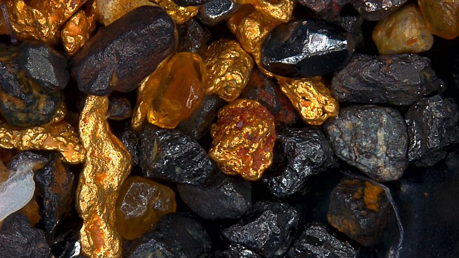
재료 분석은 재료의 물리적, 화학적 특성을 파악하기 위해 수행됩니다. 예를 들어 강철 및 알루미늄과 같은 금속 합금, 유리 및 실리콘과 같은 세라믹, 플라스틱 및 폴리머, 광물 및 지질 샘플 등이 있습니다. 재료 과학 및 지구과학은 물론 산업 품질 관리, 생산, 결함 분석, 연구 개발에 자주 사용됩니다.

기술 청정도 분석

청정도 분석은 자동차 및 전자 산업에서 제품 품질과 성능을 보증하는 데 핵심입니다. 재료 분석 현미경 솔루션은 청정도 분석 및 미립자 오염의 특성화에 중요합니다. 또한 구성 정보를 획득하면 입자를 식별한 후 오염원을 더욱 효율적으로 찾을 수 있습니다.

자세히 읽기

금속학 및 금속공학

강철의 비금속 개재물 검사부터 입자 및 상 분석 요구 사항에 이르기까지, 재료 분석을 위한 고성능 현미경은 제조업체가 원하는 특성을 가진 합금을 빠르고 안정적으로 개발할 수 있도록 도와줍니다. 유연하고 합리적인 가격의 재료 분석 현미경 솔루션은 워크플로우 및 생산 공정의 지속적인 최적화를 위해 통계적으로 유의미한 데이터의 효율적인 획득을 통해 비용을 절감합니다.

자세히 읽기

예술품 보존

디지털카메라 기술 및 이미지 분석 소프트웨어와 결합된 라이카마이크로시스템즈의 미술 작품 보존 현미경 솔루션은 복원, 유적지, 고고학자 및 재료 보존 연구소와 박물관 전문가들의 다양한 활동 분야를 위해 설계되었습니다.

자세히 읽기

강철 품질 평가

비금속 개재물로 알려진 강철의 이물질은 미세 구조의 균질성을 떨어트립니다. 이로 인해 강철의 기계적 특성이 상당한 영향을 받으므로 성능과 수명에도 영향을 줄 수 있습니다. 비금속 개재물 평가가 강철 품질을 평가하는 데 중요한 이유입니다.

자세히 읽기

Scroll to top