DM12000 M
Microscopes droits
Microscopie optique
Produits
Accueil
Leica Microsystems
DM12000 M Contrôle de précision de 12 po et système de révision
Lire nos derniers articles

Visualizing Photoresist Residue and Organic Contamination on Wafers
As the scale of integrated circuits (ICs) on semiconductors passes below 10 nm, efficient detection of organic contamination, like photoresist residue, and defects during wafer inspection is becoming…
 at the edge of a battery electrode acquired with a DVM6 digital microscope.")
Burr Detection During Battery Manufacturing
See how optical microscopy can be used for burr detection on battery electrodes and determination of damage potential to achieve rapid and reliable quality control during battery manufacturing.
 and oblique (right) brightfield illumination using a Leica compound microscope. The defect on the wafer surface is clearly more visible with oblique illumination.")
Rapid Semiconductor Inspection with Microscope Contrast Methods
Semiconductor inspection for QC of materials like wafers can be challenging. Microscope solutions that offer several contrast methods enable fast and reliable defect detection and efficient workflows.

How to Boost your Microelectronic Component Inspection Performance
Do you need to see more when inspecting silicon wafers or MEMS? Would you like to get sharp and detailed sample images which are similar to those from electron microscopes?
Watch this free webinar…
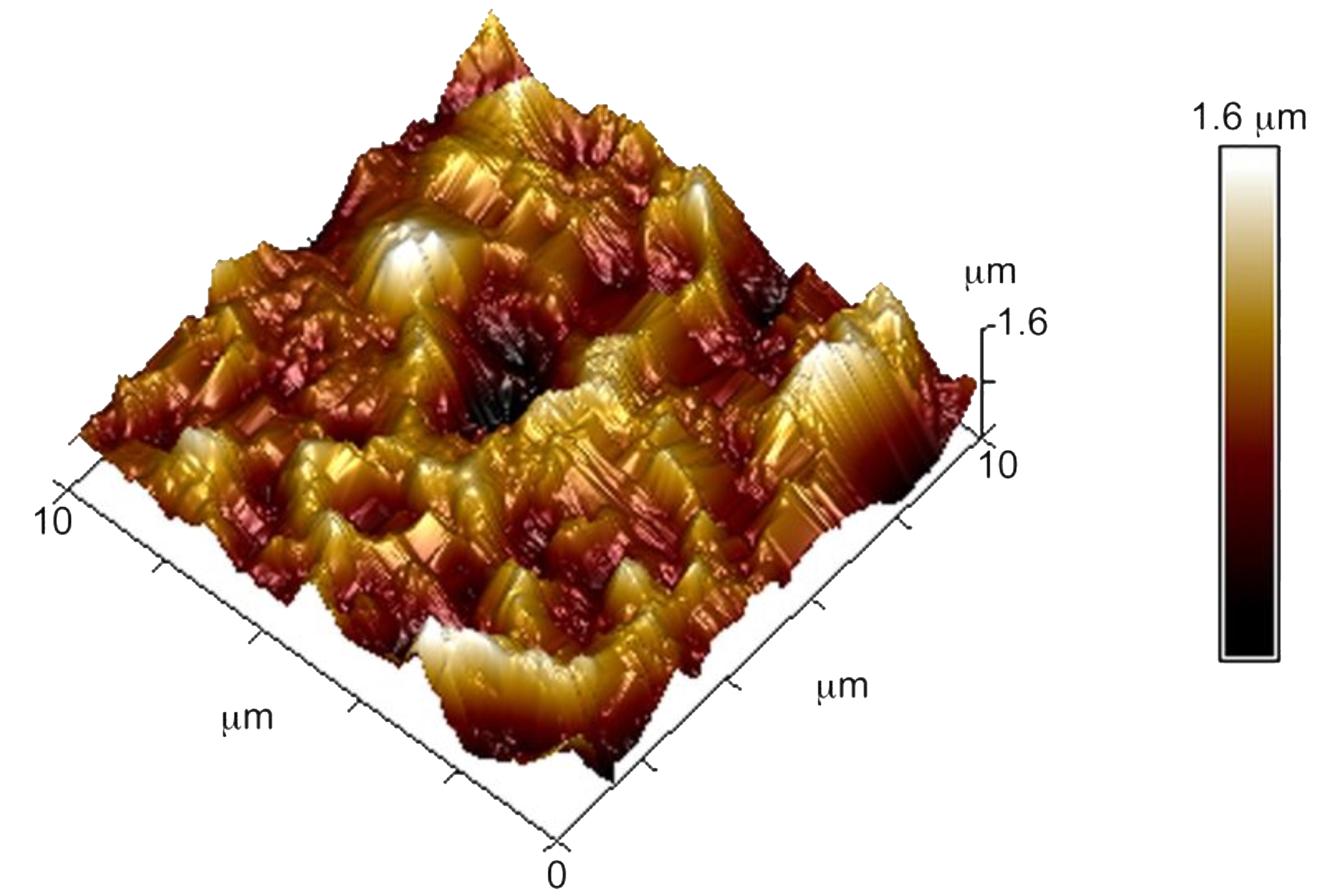
Brief Introduction to Surface Metrology
This report briefly discusses several important metrology techniques and standard definitions commonly used to assess the topography of surfaces, also known as surface texture or surface finish. With…
Domaines d'application
Inspection des semi-conducteurs
Réalisez une inspection rapide et fiable des plaquette et des semi-conducteurs pour le traitement des plaquettes, ainsi que le conditionnement, l’assemblage et les tests des circuits intégrés, avec…
Marchés de la microscopie industrielle
L'optimisation du temps de fonctionnement et la réalisation efficace des objectifs contribuent à votre résultat net. Les solutions de microscopie de Leica peuvent vous donner un aperçu des plus petits…