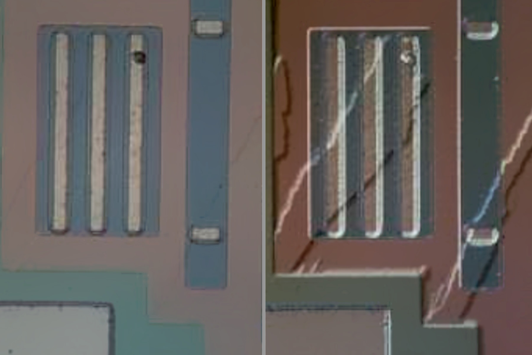
 and oblique (right) brightfield illumination using a Leica compound microscope. The defect on the wafer surface is clearly more visible with oblique illumination.")
What you can expect from this article: rapid semiconductor inspection
A Guide to Microscope Contrast Methods
The pursuit of quality in semiconductor manufacturing requires a keen eye for detail. This guide explores the critical role of microscopy, specifically the power of various contrast methods, in identifying and minimizing defects during the production of patterned wafers and integrated circuits (ICs).
This guide is a valuable resource for those seeking to attain defect-free chip manufacturing. By harnessing the power of microscopy and its various contrast methods, manufacturers can achieve new levels of quality and reliability in their ICs.

. With DIC users are able to visualize small height differences on the wafer surface more easily.")

