Contact Us

James DeRose , Ph.D.

James DeRose

James DeRose is a Global Marketing Communication Manager at Leica Microsystems. His focus is on optimized content creation for applications concerning life science, material science, as well as industry and manufacturing. He is involved with application notes, case studies, technical reports, white papers, application pages, product pages, social media posts, emails, testimonials, and other materials. He has worked at Leica Microsystems since 2013. In the past, he worked on applications development projects in the fields of interfacial chemistry and physics, thermal and chemical engineering, corrosion and metallography, surface coatings, materials science, biotechnology, and cellular biology. He has expertise with various types of microscopy and analytical methods.

Image of confluent cells taken with phase contrast (left) and analyzed for confluency using AI (right).

AI Confluency Analysis for Enhanced Precision in 2D Cell Culture

This article explains how efficient, precise confluency assessment of 2D cell culture can be done with artificial intelligence (AI). Assessing confluency, the percentage of surface area covered,…
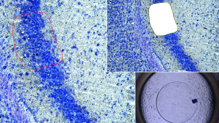
Image of murine dopaminergic neurons which have been marked for laser microdissection (LMD).

Neuron Isolation in Spatial Context with Laser Microdissection (LMD)

After Alzheimer’s disease, Parkinson’s is the second most common progressive neurodegenerative disease. Before the first symptoms manifest, up to 70% of dopamine-releasing neurons in the mid-brain…
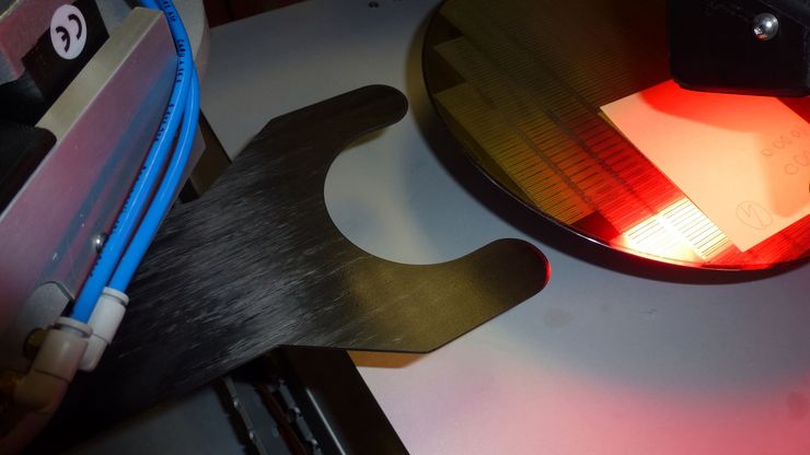
Region of a patterned wafer inspected using optical microscopy and automated and reproducible DIC (differential interference contrast). With DIC users are able to visualize small height differences on the wafer surface more easily.

6-Inch Wafer Inspection Microscope for Reliably Observing Small Height Differences

A 6-inch wafer inspection microscope with automated and reproducible DIC (differential interference contrast) imaging, no matter the skill level of users, is described in this article. Manufacturing…
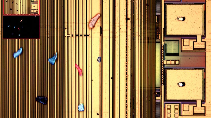
Optical microscope image, which is a composition of both brightfield and fluorescence illumination, showing organic contamination on a wafer surface. The inset images in the upper left corner show the brightfield image (above) and fluorescence image (below with dark background).

Visualizing Photoresist Residue and Organic Contamination on Wafers

As the scale of integrated circuits (ICs) on semiconductors passes below 10 nm, efficient detection of organic contamination, like photoresist residue, and defects during wafer inspection is becoming…
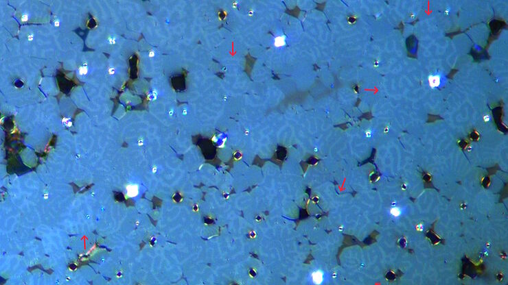
Image of burrs (red arrows) at the edge of a battery electrode acquired with a DVM6 digital microscope.

Burr Detection During Battery Manufacturing

See how optical microscopy can be used for burr detection on battery electrodes and determination of damage potential to achieve rapid and reliable quality control during battery manufacturing.
Particles observed on the surface of a particle trap which could be used for technical cleanliness during battery production.

Battery Particle Detection During the Production Process

How battery particle detection and analysis is enhanced with optical microscopy and laser spectroscopy for rapid, reliable, and cost-effective QC during battery production is explained in this…
THUNDER image of brain-capillary endothelial-like cells derived from human iPSCs (induced pluripotent stem cells) where cyan indicates nuclei and magenta tight junctions.

Rapid Check of Live Stem Cells in Cell-Culture Inserts set in Multi-Well Plates

See how efficient imaging of live iPSC stem cells within cell-culture inserts set in a multi-well plate can be done to evaluate the cells using a THUNDER Imager. Just read this article.
Particulate contamination in between moving metal plates.

Key Factors for Efficient Cleanliness Analysis

An overview of the key factors necessary for technical cleanliness and efficient cleanliness analysis concerning automotive and electronics manufacturing and production is provided in this article.
Microscope equipped with a K7 color CMOS camera for life-science and industry imaging applications.

Technical Terms for Digital Microscope Cameras and Image Analysis

Learn more about the basic principles behind digital microscope camera technologies, how digital cameras work, and take advantage of a reference list of technical terms from this article.
Images of the same area of a processed wafer taken with standard (left) and oblique (right) brightfield illumination using a Leica compound microscope. The defect on the wafer surface is clearly more visible with oblique illumination.

Rapid Semiconductor Inspection with Microscope Contrast Methods

Semiconductor inspection for QC of materials like wafers can be challenging. Microscope solutions that offer several contrast methods enable fast and reliable defect detection and efficient workflows.
Preparation of an IC-chip cross section: grinding and polishing of the chip cross section.

Cross-section Analysis for Electronics Manufacturing

This article describes cross-section analysis for electronics concerning quality control and failure analysis of printed circuit boards (PCBs) and assemblies (PCBAs), integrated circuits (ICs), etc.

Studying Virus Replication with Fluorescence Microscopy

The results from research on SARS-CoV-2 virus replication kinetics, adaption capabilities, and cytopathology in Vero E6 cells, done with the help of fluorescence microscopy, are described in this…
Image of a Siemens star, where the diameter of the 1st black line circle is 10 mm and the 2nd is 20 mm, taken via an eyepiece of a M205 A stereo microscope. The rectangles represent the field of view (FOV) of a Leica digital camera when installed with various C-mounts (red 0.32x, blue 0.5x, green 0.63x).

Understanding Clearly the Magnification of Microscopy

To help users better understand the magnification of microscopy and how to determine the useful range of magnification values for digital microscopes, this article provides helpful guidelines.
Fluorescence microscopy image of liver tissue where DNA in the nuclei are stained with Feulgen-pararosanilin and visualized with transmitted green light.

Epi-Illumination Fluorescence and Reflection-Contrast Microscopy

This article discusses the development of epi-illumination and reflection contrast for fluorescence microscopy concerning life-science applications. Much was done by the Ploem research group…
Image of an onion flake taken with a basic Leica compound microscope after it was tested for resistance to fungus and mold growth following part 11 of the ISO 9022 standard.

ISO 9022 Standard Part 11 - Testing Microscopes with Severe Conditions

This article describes a test to determine the robustness of Leica microscopes to mold and fungus growth. The test follows the specifications of the ISO 9022 part 11 standard for optical instruments.
EBSD grain size distribution of the cross section of a gold wire within a silicon matrix from inside a CPU (central processing unit of a computer). The grains are highlighted with arbitrary colors.

High-Quality EBSD Sample Preparation

This article describes a method for EBSD sample preparation of challenging materials. The high-quality samples required for electron backscatter diffraction are prepared with broad ion-beam milling.
Stereo microscopes are often considered the workhorses of laboratories and production sites.

Key Factors to Consider When Selecting a Stereo Microscope

This article explains key factors that help users determine which stereo microscope solution can best meet their needs, depending on the application.

Rapid and Reliable Examination of PCBs & PCBAs with Digital Microscopy

Digital microscopes provide users with a convenient and rapid way to acquire high-quality, reliable image data and make quick inspection and analysis of printed circuit boards (PCBs) and assemblies…
Scroll to top