Medical Device Quality Assurance and Quality Control

医療機器QAおよびQCのための顕微鏡ソリューション

医療機器、特にリスクの高いクラスIIおよびIIIの埋め込み型機器(ステント、歯科用インプラント、カテーテルなど)には、品質保証/品質管理において精密な検査が不可欠です。ライカのソリューションは、欠陥の特定、分析、文書化を効率的に行い、同時に規制要件への準拠を保証します。

ライカに問合せする

詳細説明などご希望の場合は、弊社までお問い合わせください。

アプリケーションの分野を選択してください。
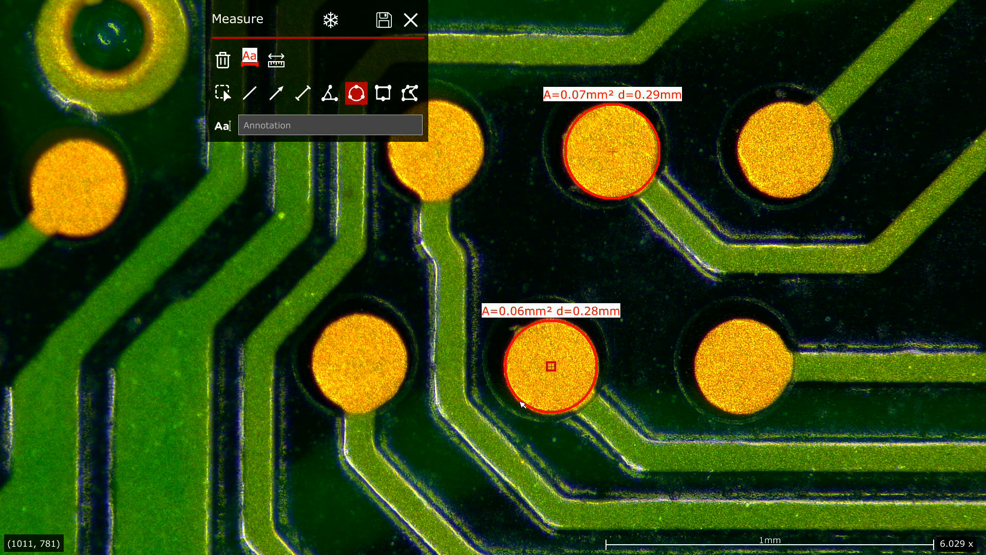
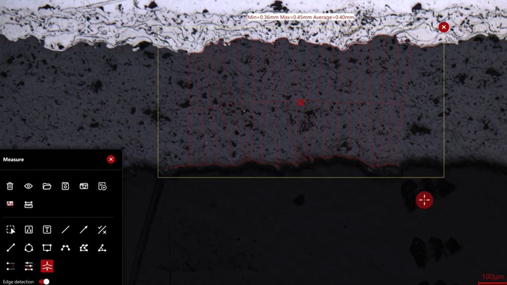
微小な欠陥を確実に検出するには?

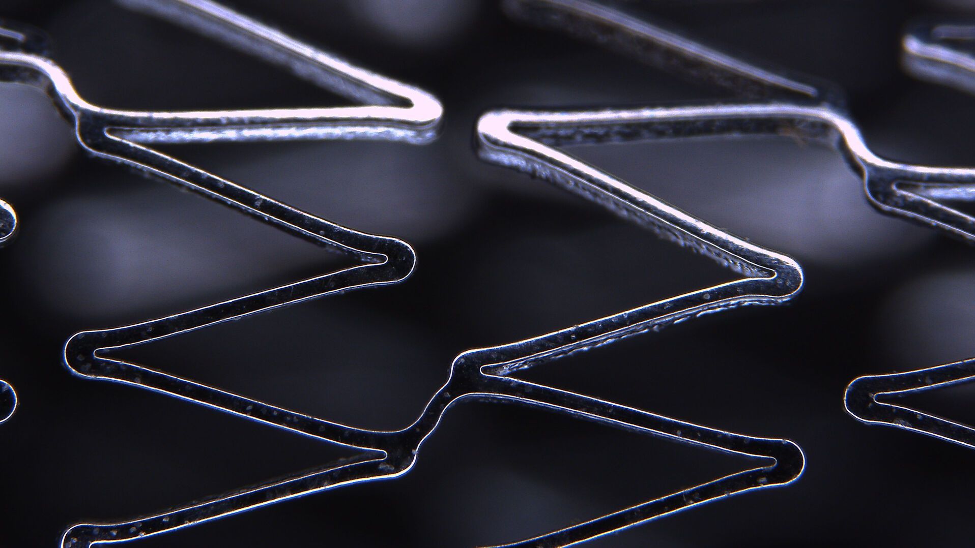
適切な解像度と照明を備えた光学顕微鏡を使用することで、医療機器の亀裂やその他の表面の凹凸などの欠陥を正確に検出し、測定することができます。Leicaの実体顕微鏡には、幅広い照明オプションが用意されています。FusionOpticsテクノロジーにより、立体観察で細かい欠陥も見逃さず観察できます。
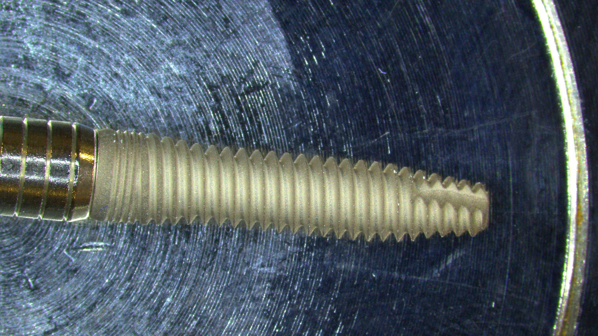
不規則な形状の機器を検査するには?

不規則な形状のデバイスを検査するために深い焦点深度と適切な作動距離を併せ持つ顕微鏡が必要です。最大122mmの作動距離を持つIvesta 3実体顕微鏡で、大きなサンプルや不規則な形状のサンプルの詳細な検査を可能にします。

目視検査中の疲労を避けるには?

人間工学に基づいて設計された顕微鏡ワークステーションを使用することで、作業による疲労や緊張が軽減され、ユーザーの作業環境を改善、集中力を向上させることで、作業の質の向上につながります。Leica実体顕微鏡用の人間工学に基づいたアクセサリーは、長時間の作業でも快適に作業することができます。
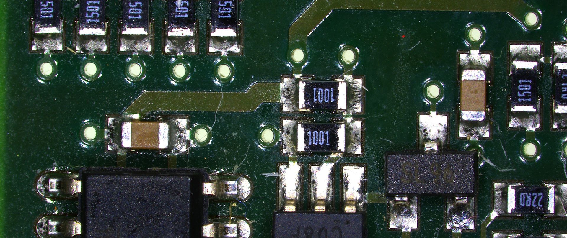
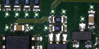
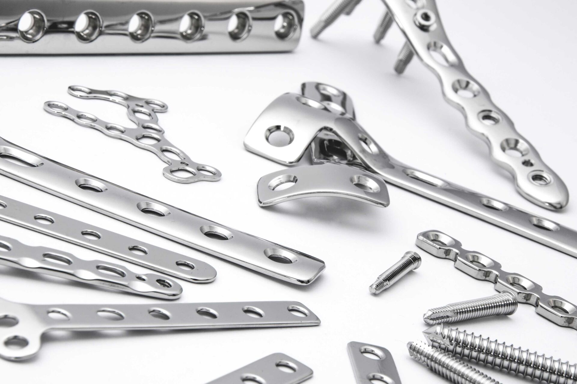
複合材料サンプルの目視検査方法は?

医療機器は複数の材料(金属やプラスチックなど)から構成されることがあります。材料の種類によって、検査時に必要な照明の種類は異なります。Leicaの顕微鏡は幅広い照明オプションを提供し、エッジや表面欠陥を効率的に観察することができます。

Leicaの顕微鏡は、医療機器の品質保証/品質管理の向上にどのように役立っていますか?


品質管理プロセスのスピードアップ

Leica の顕微鏡専用のLeica LAS X for Industry や Enersight ソフトウェアは、医療機器の検査に最適です。LAS Xの各種モジュールは、測定、画像解析の自動化、レポートアウトまでを可能にします。Enersightは使いやすいインターフェースで、検査のスピードアップに役立つ測定ツールや機能を備えています。


不定形デバイスの検査

Leica FusionOptics テクノロジー搭載の実体顕微鏡は、被写界深度が深く、解像度の高い画像を観察・取得できるため、重要な部位も見逃さず確認することができます。ステントやカテーテルのような不規則な形状の器具の検査が簡単になります。


人間工学デザインで快適な作業

Mシリーズ実体顕微鏡には、人間工学に基づいた様々なアクセサリーがあります。デジタルマイクロスコープは、サンプル画像をモニターに表示します。ユーザーは、楽な姿勢でモニター上で確認し分析できます。さまざまなユーザーのニーズに対応できるよう、うまく設計された職場環境でパフォーマンスを向上させることができます。

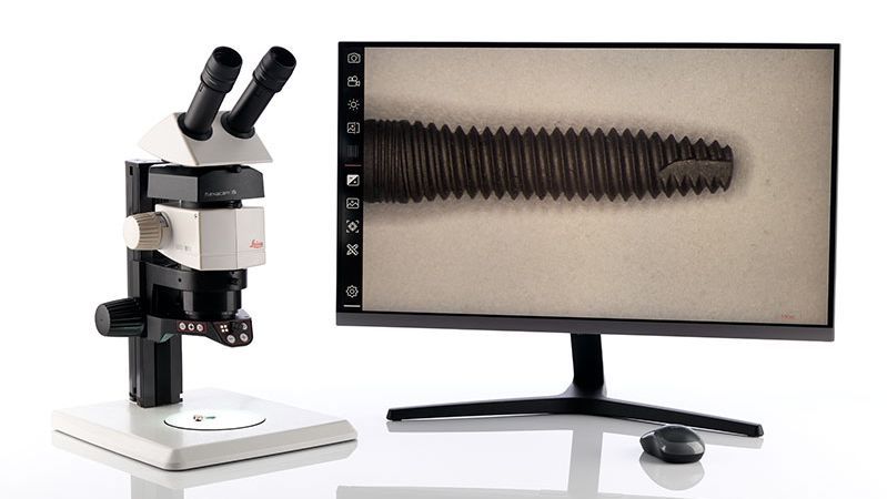
よくある質問 医療機器の品質保証と品質管理 顕微鏡ソリューション
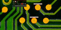
関連記事

医療機器の品質保証と品質管理に関する最新記事を読む

ライカ マイクロシステムズの知識ポータルでは、顕微鏡に関する科学的な研究記事および教材を提供しています。日常業務や研究で、ビギナーの方から経験豊富な方まで幅広くサポートします。

その他の記事
Some 2D measurements, e.g., lengths and areas, made on a PCB sample with a Leica measurement microscope using the Enersight software.

How to Select the Right Measurement Microscope

With a measurement microscope, users can measure the size and dimensions of sample features in both 2D and 3D, something crucial for inspection, QC, failure analysis, and R&D. However, choosing the…
Example of calibrating a microscope at a higher magnification value using a stage micrometer.

Microscope Calibration for Measurements: Why and How You Should Do It

Microscope calibration ensures accurate and consistent measurements for inspection, quality control (QC), failure analysis, and research and development (R&D). Calibration steps are described in this…
Optical microscope image, which is a composition of both brightfield and fluorescence illumination, showing organic contamination on a wafer surface. The inset images in the upper left corner show the brightfield image (above) and fluorescence image (below with dark background).

Visualizing Photoresist Residue and Organic Contamination on Wafers

As the scale of integrated circuits (ICs) on semiconductors passes below 10 nm, efficient detection of organic contamination, like photoresist residue, and defects during wafer inspection is becoming…
Image of magnetic steel taken with a 100x objective using Kerr microscopy. The magnetic domains in the grains appear in the image with lighter and darker patterns. A few domains are marked with red arrows. Courtesy of Florian Lang-Melzian, Robert Bosch GmbH, Germany.

Rapidly Visualizing Magnetic Domains in Steel with Kerr Microscopy

The rotation of polarized light after interaction with magnetic domains in a material, known as the Kerr effect, enables the investigation of magnetized samples with Kerr microscopy. It allows rapid…
Region of a patterned wafer inspected using optical microscopy and automated and reproducible DIC (differential interference contrast). With DIC users are able to visualize small height differences on the wafer surface more easily.

6-Inch Wafer Inspection Microscope for Reliably Observing Small Height Differences

A 6-inch wafer inspection microscope with automated and reproducible DIC (differential interference contrast) imaging, no matter the skill level of users, is described in this article. Manufacturing…
Automated wafer loader using carbon fiber end-effectors for safer handling.

Safe Wafer Loading for Microscope Inspection without Hand Contact

How automated silicon wafer loading for microscope inspection helps improve microelectronics process control and production efficiency is explained in this article. Manual handling of wafers has a…
Image of burrs (red arrows) at the edge of a battery electrode acquired with a DVM6 digital microscope.

Burr Detection During Battery Manufacturing

See how optical microscopy can be used for burr detection on battery electrodes and determination of damage potential to achieve rapid and reliable quality control during battery manufacturing.
Quality assurance during production in a manufacturing plant.

Quality Assurance Improvement Across Industries

Precision is paramount. Imagine a pacemaker that fails mid-operation or a semiconductor flaw that causes a critical system crash. In industries, such as medical devices, electronics, and…
Radially grown sugar crystals which have been imaged with a Leica microscope using circular polarized light.

Polarizing Microscope Image Gallery

How polarization microscope images can be used for analysis is shown in this gallery. Polarized light microscopy (also known as polarizing microscopy) is an important method for different fields and…
SEM image of the full Li-NMC electrode sample, showing the two porous layers and the metal film at the center of the structure.

Revealing Sodium Battery Degradation via Cryo-EM and CryoFIB

Explore how cryogenic electron microscopy and focused ion beam techniques uncover the intrinsic structure of sodium battery interfaces. This webinar presents a new degradation model based on separator…
面積と距離の測定

測定

光学顕微鏡は、品質管理、故障解析、研究開発において、試料の形状寸法測定にも役立ちます。ライカの光学顕微鏡の詳細をご覧ください。

もっと読む

検査用顕微鏡

ライカの検査用顕微鏡は、構成部品やサンプル全体像の把握から細部の確認まで、あらゆるニーズに対応します。

もっと読む

組立・リワークの検査

ライカマイクロシステムズの人間工学に基づいた顕微鏡ソリューションで、精度とスピードを実現し、生産性を最大限に高め、高品質な結果を簡単に得ることができます。優れた光学品質と広い視野を誇るこれらのシステムは、組立やリワークのワークフローを最適化しながら、オペレーターの快適性を保証します。

もっと読む

工業用アプリケーション

顕微鏡のライカマイクロシステムズは、無駄の軽減、仕事のクオリティ向上に役立つ製品の開発に取り組んでいます。生産活動におけるさまざまな対象物を正確に認識・理解し、効率的にレポート作成していただけるよう、幅広い製品ラインナップの中から、 お客様のワークフローに最適な製品をご提案致します。

もっと読む

面積と距離の測定
Scroll to top