EM TXP
電顕用試料作製装置
製品紹介
Home
Leica Microsystems
EM TXP 断面試料作製装置
電子顕微鏡および光学顕微鏡による検査に向けた断面試料作製の出発点となる装置です。
最新の記事を読む
Workflow Solutions for Sample Preparation Methods for Material Science
This brochure presents and explains appropriate workflow solutions for the most frequently required sample preparation methods for material science samples.

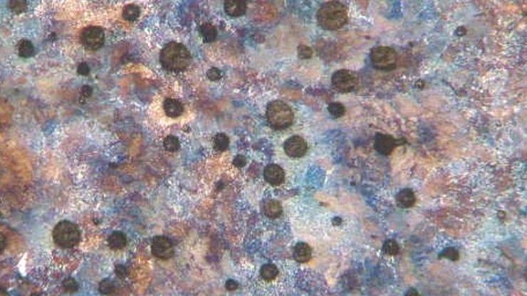
Quality Control via Cross Sections of PCBs, PCBAs, ICs, and Batteries
Why cross sections of printed circuit boards (PCBs) and assemblies (PCBAs), integrated circuits (ICs), and battery components are useful for quality control (QC), failure analysis (FA), and research…
 chip cross section acquired at higher magnification showing a region of interest.")
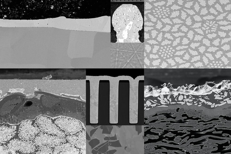
Structural and Chemical Analysis of IC-Chip Cross Sections
This article shows how electronic IC-chip cross sections can be efficiently and reliably prepared and then analyzed, both visually and chemically at the microscale, with the EM TXP and DM6 M LIBS…
. The grains are highlighted with arbitrary colors.")
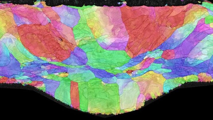
High-Quality EBSD Sample Preparation
This article describes a method for EBSD sample preparation of challenging materials. The high-quality samples required for electron backscatter diffraction are prepared with broad ion-beam milling.

How to Prepare and Analyse Battery Samples with Electron Microscopy
This workshop covers the sample preparation process for lithium and novel battery sample analysis, as well as other semiconductor samples requiring high-resolution cross-section imaging.

Cross Section Ion Beam Milling of Battery Components
Sample Preparation of Lithium battery systems requires high quality surface preparation to evaluate their internal structure and morphology. Due to the brittle materials involved, preparing pristine…
Ion Beam Milling Guide: Enhancing Surface Quality for High-Resolution Imaging and Analysis
In this article you can learn how to optimize the preparation quality of your samples by using the ion beam etching method with the EM TIC 3X ion beam milling machine. A short introduction of the…
マテリアルサイエンス& 分析
マテリアルサイエンス & 分析では、顕微鏡が重要な役割を果たします。金属合金、セラミックス、ポリマーの研究や品質管理のための分析に使用されます。
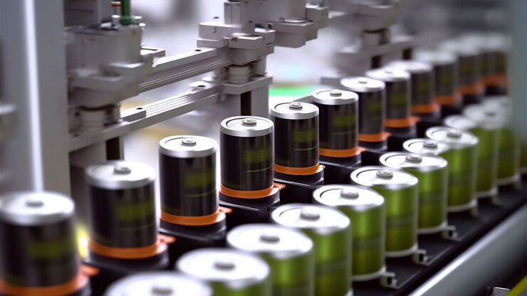
バッテリー製造
バッテリー製造には、検査に関するいくつかの主な課題があります。サンプル前処理と顕微鏡による外観検査および拡張分析用のソリューションが必要です。

金属組織分析
ライカの金属顕微鏡ソリューションを活用することで、 金属、合金、その他の材料の微細構造分析をより効率的かつ高精度に行うことができます。
Fields of Application
時計産業
時計メーカーと時計産業にとって、ライカの高精度実体顕微鏡は、強力な味方。時計の精密アセンブリーを容易に行い、品質とクラフトマンシップを高い信頼性で検査するのをサポートします。
自動車&輸送機器業界
ライカのインテリジェントなイメージングソリューションは、現在および将来のニーズに対応し、お客様は技術革新に集中することができます。
インダストリーマーケット別
稼働時間を最大化し、生産性向上により、お客様の収益に貢献します。ライカの顕微鏡(マイクロスコープ)ソリューションは、微細な異物や残渣なども見逃しなく、迅速かつ信頼性の高い分析、文書化、結果報告を実現します。ライカマイクロシステムズは、幅広いソリューションとエキスパートによるサポートを提供し、さまざまなアプリケーションのニーズにお応えします。
エレクトロニクスのための断面解析
電子・エレクトロニクス業界では、断面解析により、プリント基板(PCB)、アセンブリ(PCBA)、集積回路(IC)などのコンポーネントの故障メカニズムを詳細に解析します。
エレクトロニクスおよび半導体産業
電子機器や半導体にとって、PCB、ウェハー、ICチップ、バッテリーの効率的な検査、断面解析、清浄度分析、研究開発を可能にするソリューションは極めて重要です。
バッテリー製造
バッテリー製造には、検査に関するいくつかの主な課題があります。サンプル前処理と顕微鏡による外観検査および拡張分析用のソリューションが必要です。
マテリアルサイエンス& 分析
マテリアルサイエンス & 分析では、顕微鏡が重要な役割を果たします。金属合金、セラミックス、ポリマーの研究や品質管理のための分析に使用されます。
