Leica DM8000 M
正立顕微鏡
光学顕微鏡
製品紹介
Home
Leica Microsystems
Leica DM8000 M 半導体検査顕微鏡(8インチウエハ用)<br>
最新の記事を読む
 at the edge of a battery electrode acquired with a DVM6 digital microscope.")
Burr Detection During Battery Manufacturing
See how optical microscopy can be used for burr detection on battery electrodes and determination of damage potential to achieve rapid and reliable quality control during battery manufacturing.
 and oblique (right) brightfield illumination using a Leica compound microscope. The defect on the wafer surface is clearly more visible with oblique illumination.")
Rapid Semiconductor Inspection with Microscope Contrast Methods
Semiconductor inspection for QC of materials like wafers can be challenging. Microscope solutions that offer several contrast methods enable fast and reliable defect detection and efficient workflows.

How to Boost your Microelectronic Component Inspection Performance
Do you need to see more when inspecting silicon wafers or MEMS? Would you like to get sharp and detailed sample images which are similar to those from electron microscopes?
Watch this free webinar…
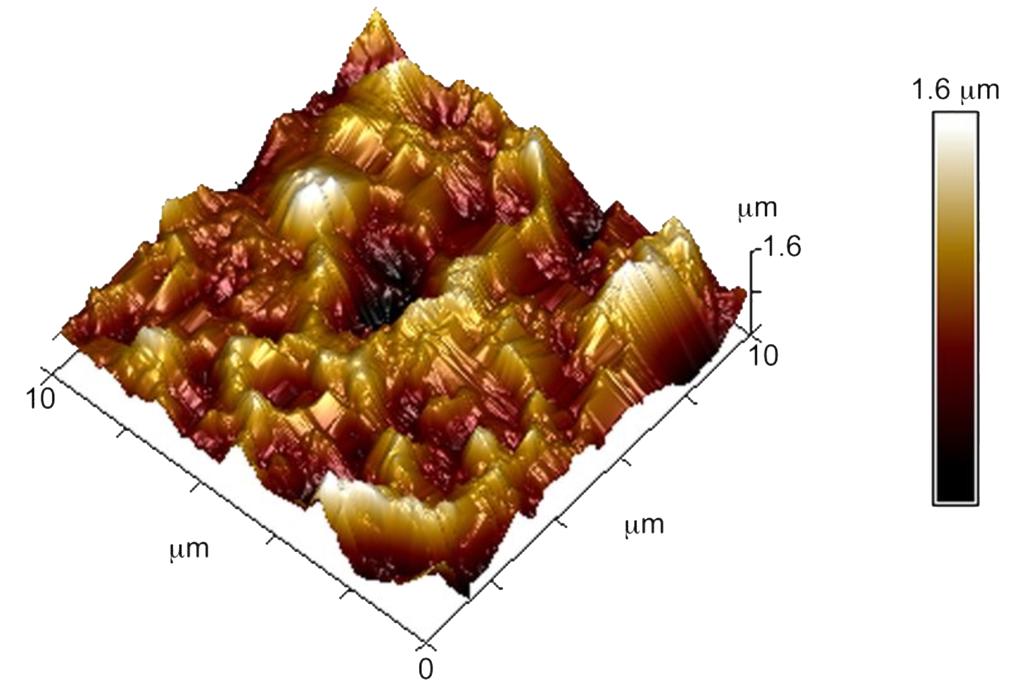
Brief Introduction to Surface Metrology
This report briefly discusses several important metrology techniques and standard definitions commonly used to assess the topography of surfaces, also known as surface texture or surface finish. With…
応用分野
半導体ウエハー処理、ICパッケージング&検査
Leica Microsystems’ customized, modular imaging solutions help suppliers and device manufacturers achieve fast and precise inspection and analysis for wafer processing, IC packaging, IC assembly, and…
工業用顕微鏡のマーケット
稼働時間を最大化し、生産性向上により、お客様の収益に貢献します。ライカの顕微鏡(マイクロスコープ)ソリューションは、微細な異物や残渣なども見逃しなく、迅速かつ信頼性の高い分析、文書化、結果報告を実現します。ライカマイクロシステムズは、幅広いソリューションとエキスパートによるサポートを提供し、さまざまなアプリケーションのニーズにお応えします。

もっと知りたいですか?
お気軽にお問合せください
ライカまでお気軽にご相談ください Show local contacts