Sciences de la vie
Sciences de la vie
C'est ici que vous pourrez développer vos connaissances, vos capacités de recherche et les applications pratiques de la microscopie dans divers domaines scientifiques. Apprenez à obtenir une visualisation précise, à interpréter les images et à faire progresser la recherche. Trouvez des informations pertinentes sur la microscopie avancée, les techniques d'imagerie, la préparation des échantillons et l'analyse des images. Les sujets abordés comprennent la biologie cellulaire, les neurosciences et la recherche sur le cancer, en mettant l'accent sur les applications et les innovations de pointe.
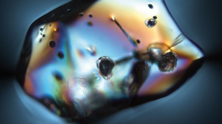
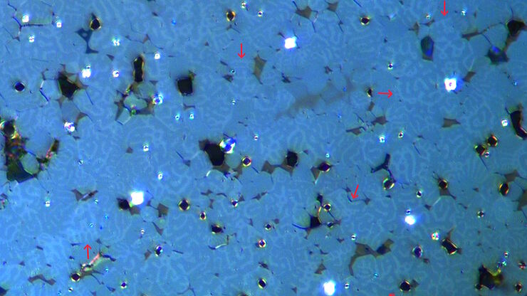
Ensuring Glass Quality with the Polarization Microscopy Advantage
Glass is one of the oldest materials known. Today, it is used for many applications, e.g., optical instruments, windows, doors, solar panels, containers for food, beverages, and medicine, so strict…
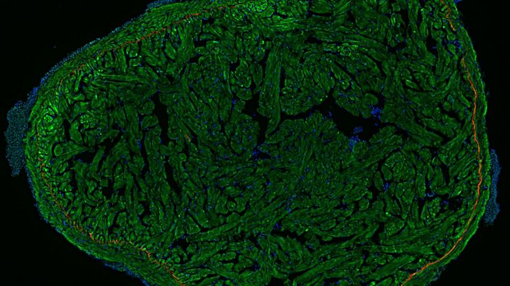
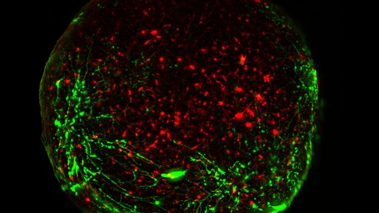
A Guide to Fluorescence Microscopy
Fluorescence microscopy uses the ability of fluorophores, dyes, or fluorescent proteins to emit light of a specific wavelength after being excited with light of a shorter wavelength. Biomolecules can…
How to Select the Right Measurement Microscope
With a measurement microscope, users can measure the size and dimensions of sample features in both 2D and 3D, something crucial for inspection, QC, failure analysis, and R&D. However, choosing the…
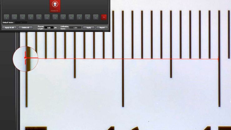
Microscope Calibration for Measurements: Why and How You Should Do It
Microscope calibration ensures accurate and consistent measurements for inspection, quality control (QC), failure analysis, and research and development (R&D). Calibration steps are described in this…
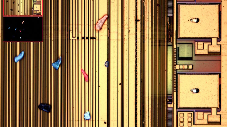
Visualizing Photoresist Residue and Organic Contamination on Wafers
As the scale of integrated circuits (ICs) on semiconductors passes below 10 nm, efficient detection of organic contamination, like photoresist residue, and defects during wafer inspection is becoming…
Rapidly Visualizing Magnetic Domains in Steel with Kerr Microscopy
The rotation of polarized light after interaction with magnetic domains in a material, known as the Kerr effect, enables the investigation of magnetized samples with Kerr microscopy. It allows rapid…
6-Inch Wafer Inspection Microscope for Reliably Observing Small Height Differences
A 6-inch wafer inspection microscope with automated and reproducible DIC (differential interference contrast) imaging, no matter the skill level of users, is described in this article. Manufacturing…
Burr Detection During Battery Manufacturing
See how optical microscopy can be used for burr detection on battery electrodes and determination of damage potential to achieve rapid and reliable quality control during battery manufacturing.
Guide to Live-Cell Imaging
For a wide range of applications in various research fields of life science, live-cell imaging is an indispensable tool for visualizing cells in a state as close to in vivo, i.e. living and active, as…
