PCB Inspection
Whether a manufacturer or supplier, efficient and reliable PCB (printed-circuit board) inspection for quality control (QC), rework, failure analysis, and research and development (R&D) is crucial for achieving cost-effective production and competitive electronic products. The performance of PCBs is critically influenced by soldering, through holes, diodes, IC chips, and other components. All of these must be checked. To show compliance with the defined specifications, an imaging solution which enables reliable and accurate documentation is often required. Inspection microscopes assist manufacturers and suppliers with their QC, failure analysis, and R&D needs.
Please contact us to get advice from Leica experts about our PCB Microscope Inspection Solutions

What is PCB Inspection and why is it important?
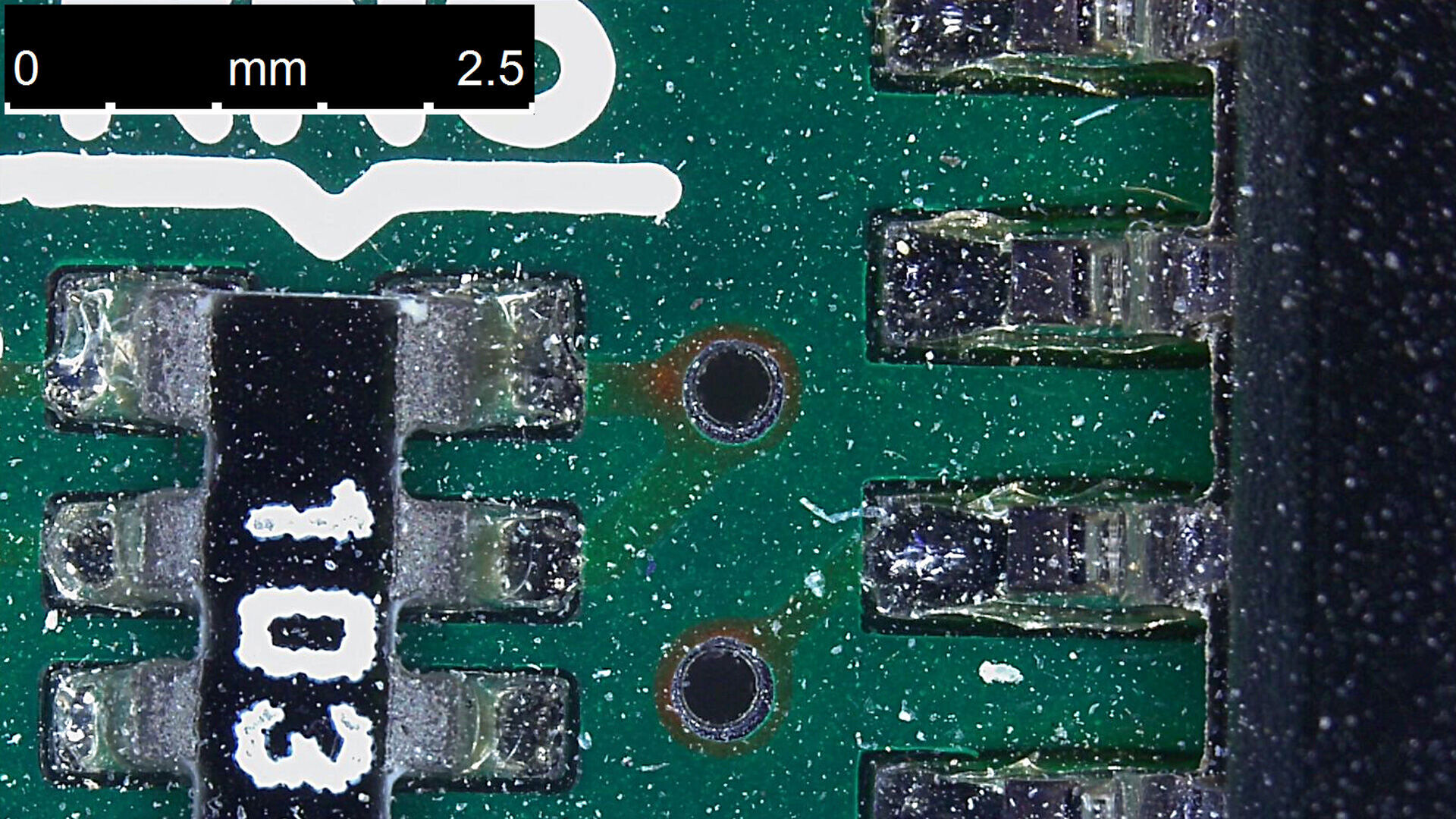
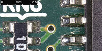
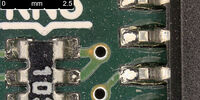
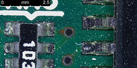
PCB (printed-circuit board) inspection is crucial for quality control, ensuring optimal performance of electronic components, and cost-effective, reliable PCB production. It is performed by doing visual inspection of boards to identify potentially damaging defects in terms of soldering, leads, component contacts, presence of particles and other contamination, during manufacturing and production.

What kinds of microscopes are used for PCB inspection?
Stereo and digital microscopes are ideal for PCB (printed-circuit board) inspection. When looking for defects or doing rework: these microscopes enable easy handling of PCSs under the objective lens, straightforward use of different types of illumination to better reveal details, and the ability to go quickly from an overview to zooming in on areas of interest. A stereo microscope with FusionOptics allows a 3D perception of the PCB while having both higher resolution and larger depth of field.

What is the best magnification for PCB inspection?
A practical magnification range for PCB (printed-circuit board) inspection with a stereo or digital microscope is 5x to 30x (including objective, zoom, and eyepieces). This range enables both a large overview of a PCB area at lower magnification (around 5x) and visualization of fine details at higher magnifications (around 25-30x).
Get the Most Suitable Inspection Solution for You Based on 2 Short Questions
Answer the short questionnaire to find the right solution for your needs. If you would rather have a Leica representative contact you, then please click here and fill out the form.
Contact us{{ question.questionText }}
Please select an answer!
Best Match
{{ resultProduct.header }}
{{ resultProduct.subheader }}
{{ resultProduct.description }}
{{ resultProduct.features }}
Request Your Information Package
Challenges for PCB Inspection
The ultimate goal for PCB inspection is ensuring and optimizing product performance and lifetime. Manufacturers and suppliers need fast and reliable inspection for screening defects and checking specifications to achieve cost-effective production.
Challenges encountered during PCB inspection with an imaging system may lead to inefficiency, reduced throughput, and higher defect-ppm rates. For example, when users are unable to:
- Find defects on PCBs quickly
- Handle PCBs easily on the imaging stage
- Focus attentively as a result of strain and discomfort during observation.
Finding defects on PCBs and checking specifications quickly requires microscope solutions which help users overcome these challenges.
Advantages of Leica PCB Inspection Microscopes
Efficient Screening of PCBs and Documentation of Results
PCB inspection should be fast and reliable. Microscope solutions should allow users to:
- See a large overview of the sample and easily zoom in on a region of interest
- Reveal more details with versatile illumination
- Handle or manipulate samples under the objective with ease due to a long working distance
- Document results in less time
- Stay comfortable and avoid strain, even when inspecting the entire day.


Image simulation, showing a printed circuit board sample without and with the FusionOptics effect, perceived when looking through the eyepieces.
Fast PCB Inspection in 3D
When a 3D perspective is important, as for handling and doing rework of PCBs, then a stereo microscope is required. Frequent microscope adjustments, e.g., refocusing and changing of zoom factor to enhance resolution and depth of field, can slow down inspection. These adjustments can be minimized with the FusionOptics technology. When looking through the eyepieces, you can perceive a PCB in 3D with both high resolution and large depth of field.
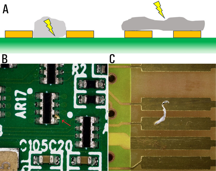
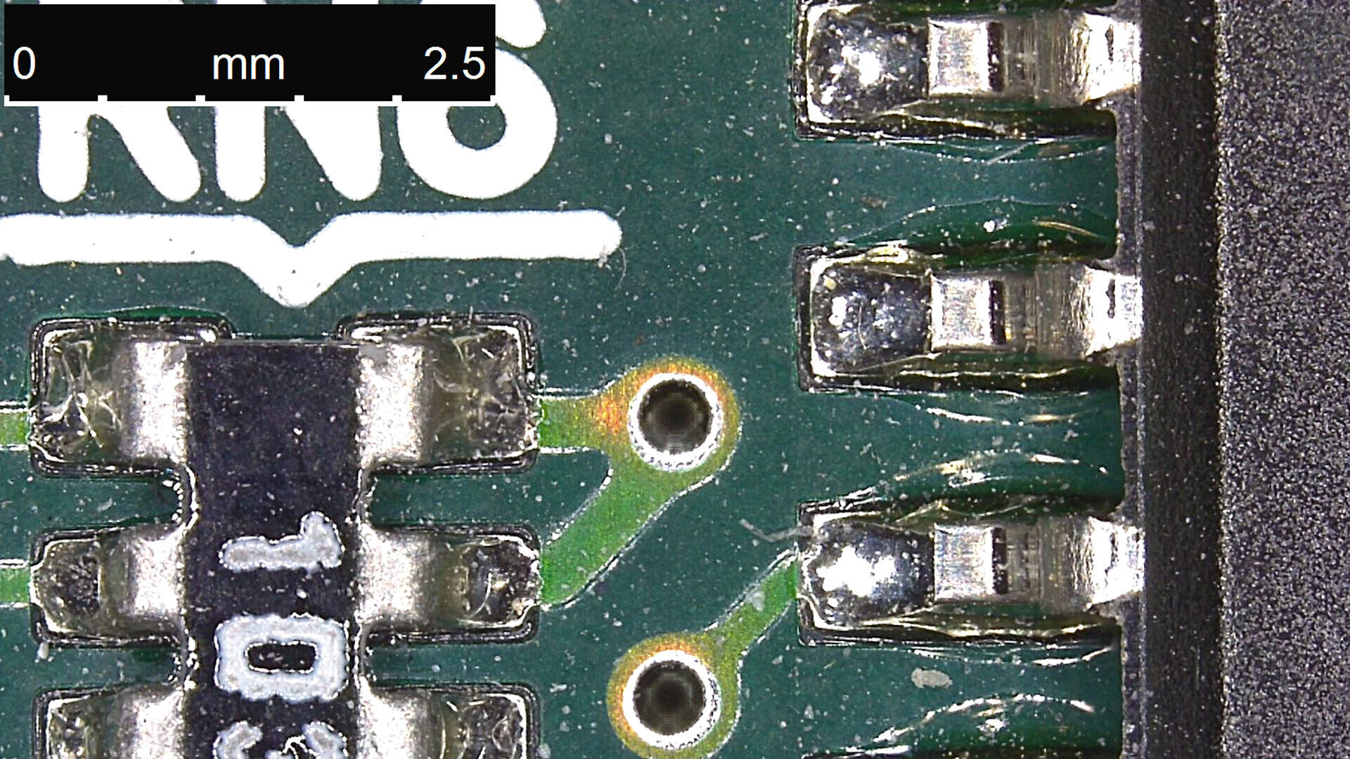
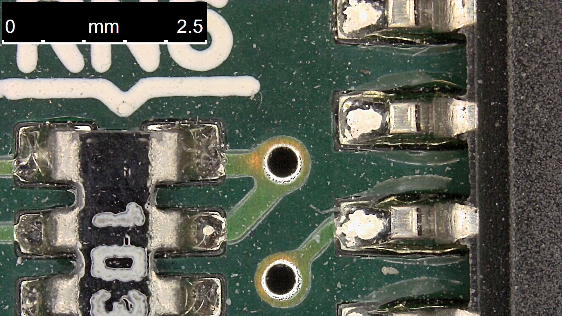
B) between leads of a PCB component
C) across leads of a PCB.
Cleanliness Analysis of PCBs
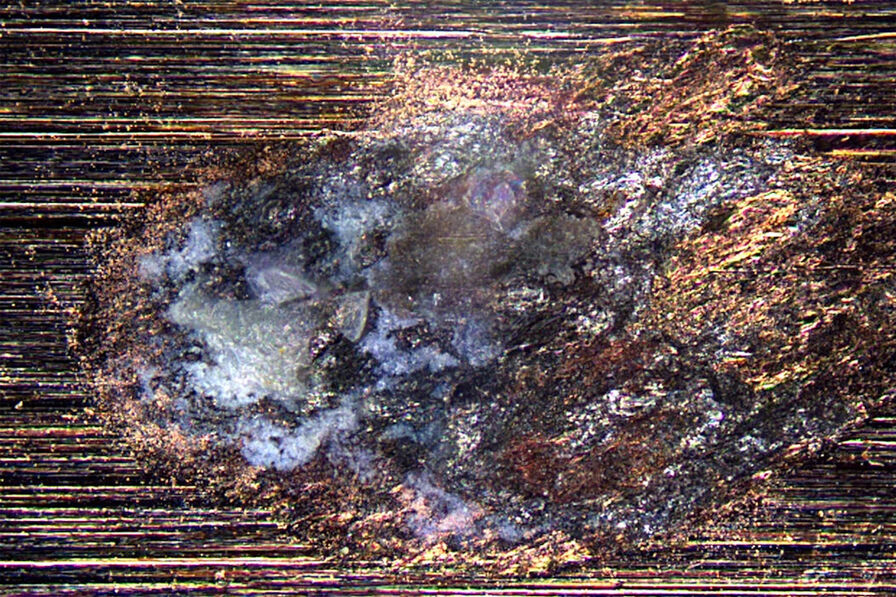
The cleanliness of PCBs is important, because small conductive particles can significantly increase the risk of failure. If these particles become present on PCBs during manufacturing, they can easily bridge small gaps between contacts and leads, causing a short circuit.
Thus, there is a need for rapid and reliable cleanliness analysis of PCBs to minimize or eliminate contamination and ensure PCB performance. The analysis involves accurate determination of particle dimensions and material following standards and guidelines like ZVEI. Cleanliness analysis can be done using an optical microscope alone or in combination with laser-induced breakdown spectroscopy (LIBS). Chemical analysis with LIBS helps to determine accurately the potential of a particle to cause short circuits and efficiently find the contamination source.
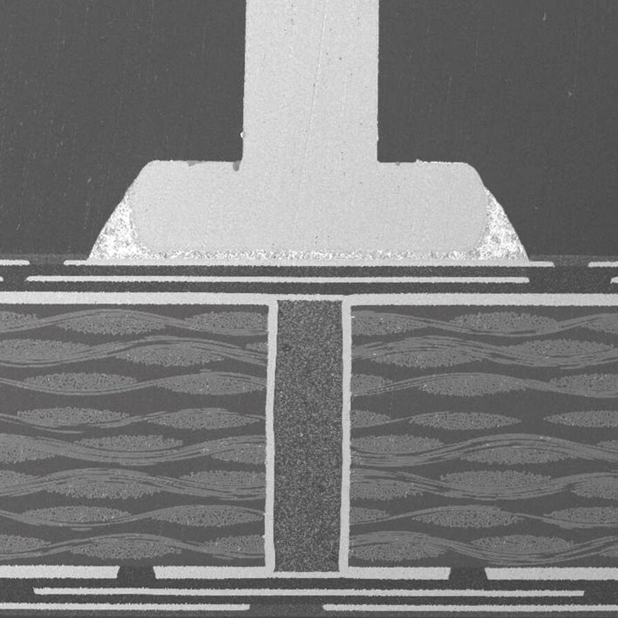
Cross-section Analysis of PCBs
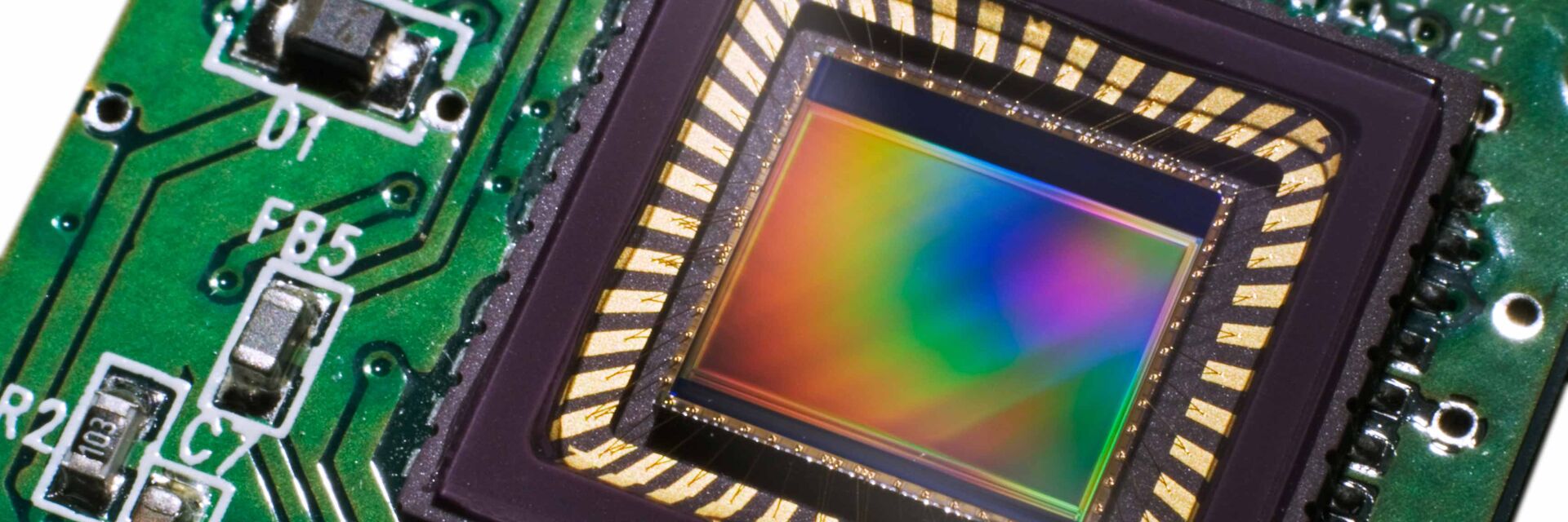
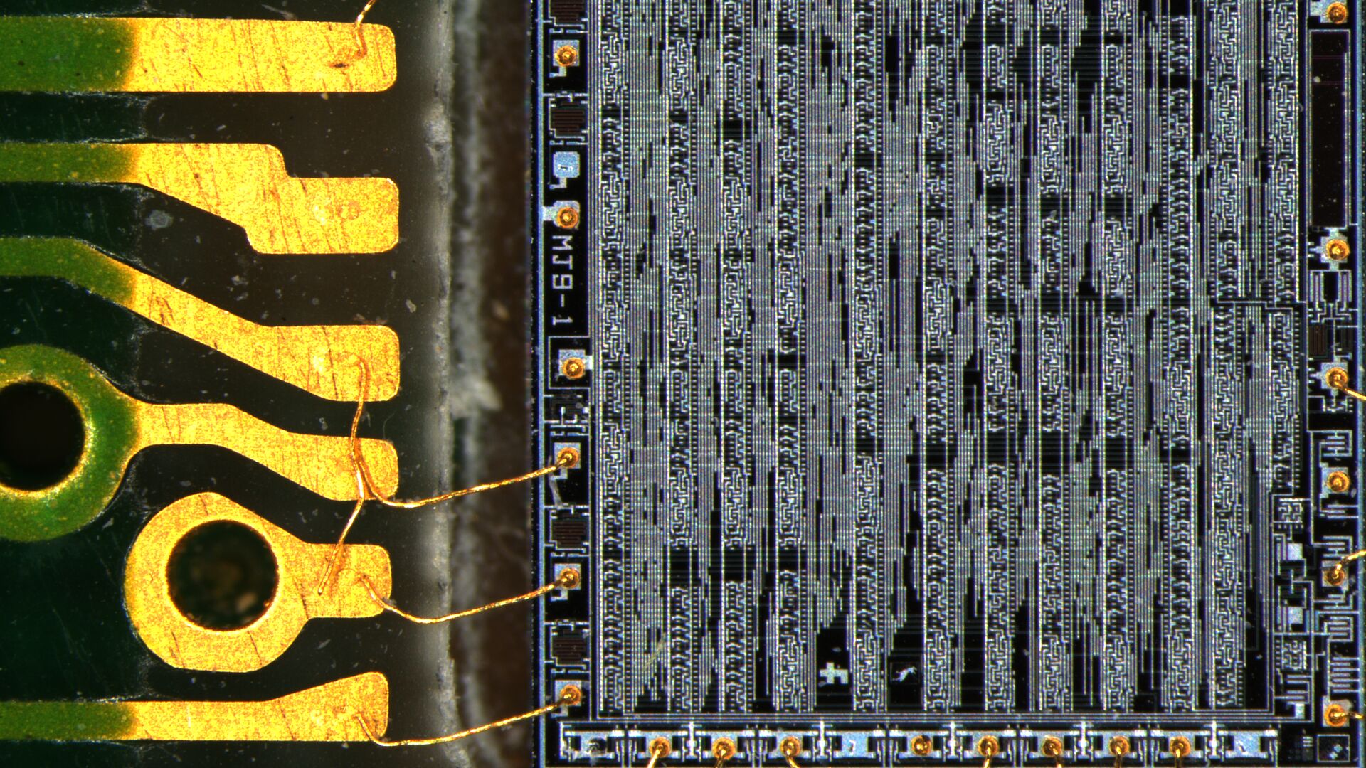
To observe the internal structure of PCBs, with the goal of identifying defects, cross sectioning is required as the materials are normally opaque. Cross-section analysis is a useful technique for QC of PCBs. It is also exploited for failure analysis and R&D. The analysis is done by cutting through a PCB and then grinding and polishing the cross section to obtain a smooth surface. Analysis of the cross section can be performed with high-resolution optical or electron microscopy and spectroscopy. The aim is to reveal the internal structure and composition of PCB layers and its components, confirm the presence or absence of coatings, vias, etc.

Electroplating of PCB Components
Electroplating is an electrochemical process used for depositing protective metallic layers, e.g., copper or tin, onto PCB interconnects or components. Defects and contamination which occur during electroplating can lead to poor electroplating quality or even PCB failure. Rapid and reliable visual inspection of electroplated components for defects can be done with optical microscopes. If a root cause analysis of defects or contamination is required, then a combination of optical microscopy and laser-induced breakdown spectroscopy (LIBS) for simultaneous visual and chemical analysis is recommended.
Frequently Asked Questions PCB Inspection
A PCB (printed circuit board) is used to assemble electronic components into a complete circuitry. They are used in electronic devices like computers, tablets, smart phones, or measurement instrumentation. PCBs are made of alternating layers of insulating and conducting materials and have holes or other ways for mounting and interconnection of electrical components onto the board. Different types of boards (single or multi-layer) and designs (blind, buried, or through-hole vias or surface mount) exist depending on the application.
When electronic components are assembled and attached, usually by soldering, onto a PCB (printed circuit board), then it becomes a PCBA (printed circuit board assembly). It is a PCBA which is actually inserted into an electronic device like a computer, tablet, smart phone, or measurement instrument.
A PCB is a printed circuit board, a bare support without electronic components simply used to assemble together components into a complete circuit. A PCBA is a printed circuit board assembly, the finished product with all the electronic components attached to the PCB and ready to be used in an electronic device.
PCBs (printed circuit boards) are used in many electronic devices. A PCB serves as a support onto which electronic components are mounted to form a complete circuitry. Once the components are installed and a PCBA (printed circuit board assembly) is finished, then it can be installed in electronic devices to perform specific tasks like data processing.
 chip cross section acquired at higher magnification showing a region of interest.")


