
Semiconductor Inspection Microscopy Solutions
Manufacturers and suppliers need to achieve fast and reliable semiconductor inspection and analysis for wafer processing as well as integrated-circuit (IC) packaging, assembly, and testing. Conformity to the defined specifications during semiconductor manufacturing is critical for reliability. The expected level of cleanliness and minimal presence of defects have to be met in order to produce high-quality semiconductor devices and IC chips. Therefore, microscope solutions for efficient wafer and semiconductor inspection are crucial to meet this aim. Additionally, the demand for higher performance technology is also unrelenting, so these microscopes should make contributions to R&D.
Please contact us for expert advice on our microscopy solutions for Semiconductor Inspection.

Why is wafer and semiconductor inspection important?
Wafer and semiconductor inspection is important during production, because it helps ensure the quality and reliability of IC chips and other electronic components. It involves detection and analysis of defects, scratches, or contamination (particles, residues, etc.) which may occur during the manufacturing process. Such defects or contamination could harm component performance, cause failure, or disrupt the smooth flow of production.

How can you achieve efficient wafer and semiconductor inspection?
Efficient visual inspection can be performed with optical microscopy using a variety of lighting and contrast methods (brightfield, darkfield, polarization, DIC, UV, oblique illumination, IR) and a range of magnifications. Various defects, scratches, and contamination on wafers and semiconductors can be quickly and reliably detected and analyzed.

Why can semiconductor inspection require cross-section analysis?
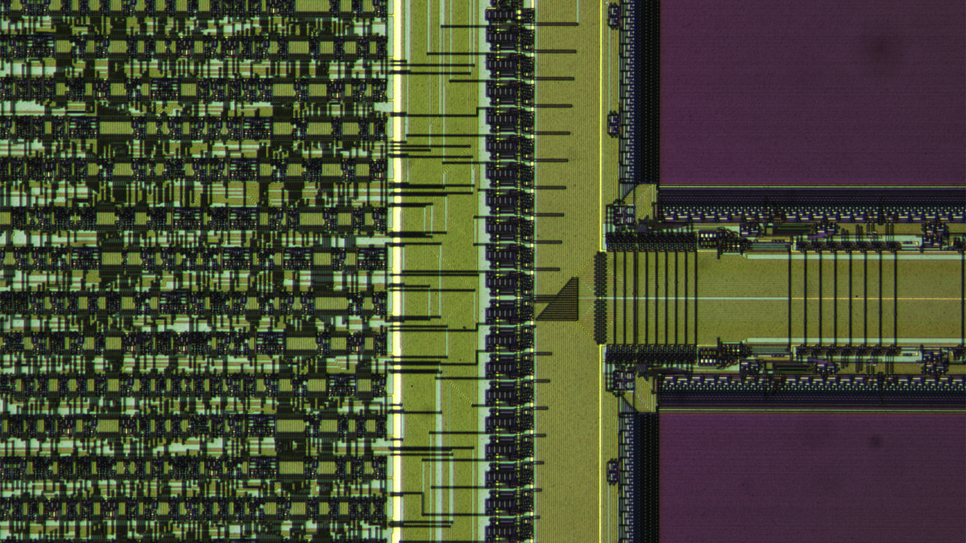
Defects can become present in the bulk material of semiconductor components, like IC (integrated-circuit) chips, during production and have an effect on component quality and reliability. To check for these defects, as the materials are often opaque, cross-section analysis is sometimes necessary. The internal structure of semiconductor components cannot be seen without first doing cross-section preparation. Then analysis is done to observe and analyze any defects that may be present in the internal structure.
Get Your Individual Solution Based on 3 Short Questions.
Dedicated configurations are available for your specific needs. Answer the short questionnaire to find the right solution for your needs. If you would rather have a representative contact you, then please click here to fill out your contact information.
Contact us{{ question.questionText }}
Please select an answer!
Best Match
{{ resultProduct.header }}
{{ resultProduct.subheader }}
{{ resultProduct.description }}
{{ resultProduct.features }}
Request Your Information Package
Challenges of Wafer and Semiconductor Inspection
When inspecting wafers and semiconductors, it can be challenging to optimize the workflow, as users should:
- Go efficiently from an overview of the wafer or semiconductor to seeing the fine details
- Visualize rapidly and reliably different types of defects, scratches, residues, contamination, etc.
- Work in a comfortable way allowing an enhanced inspection performance.
These inspection challenges can be overcome with the appropriate microscope solutions.
See More With Diverse Contrast Methods
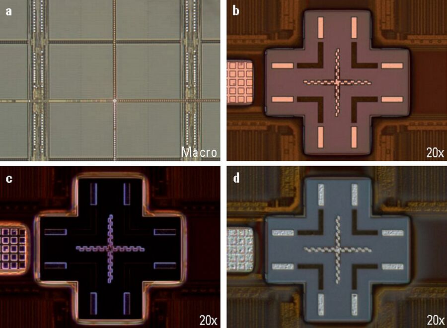
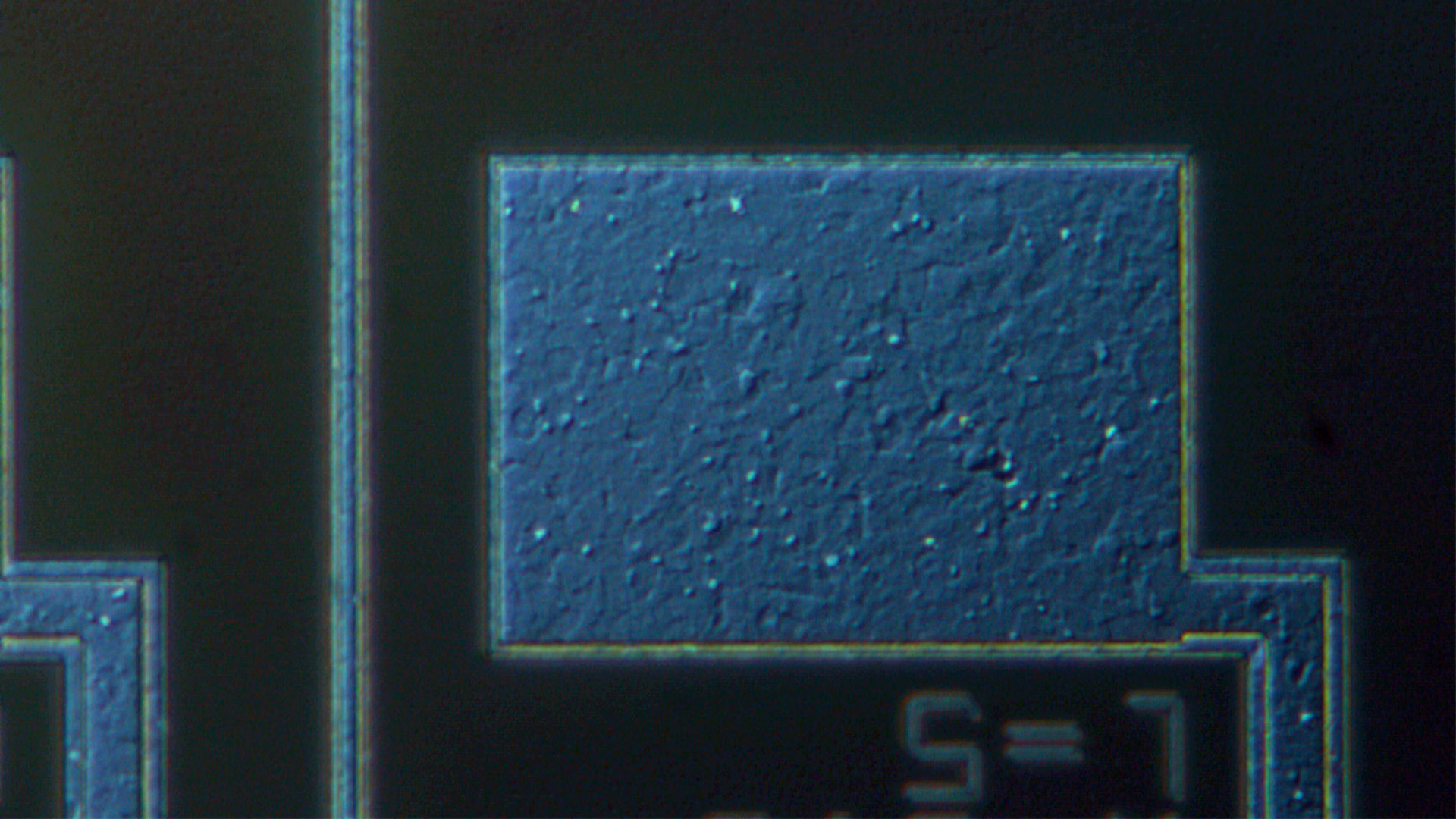
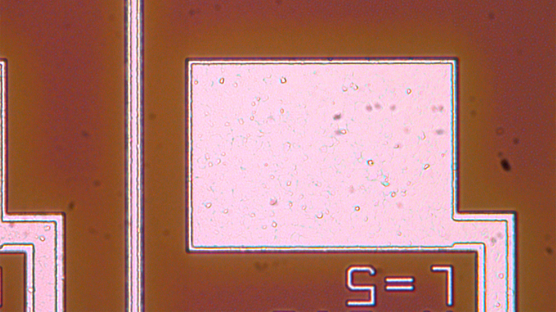
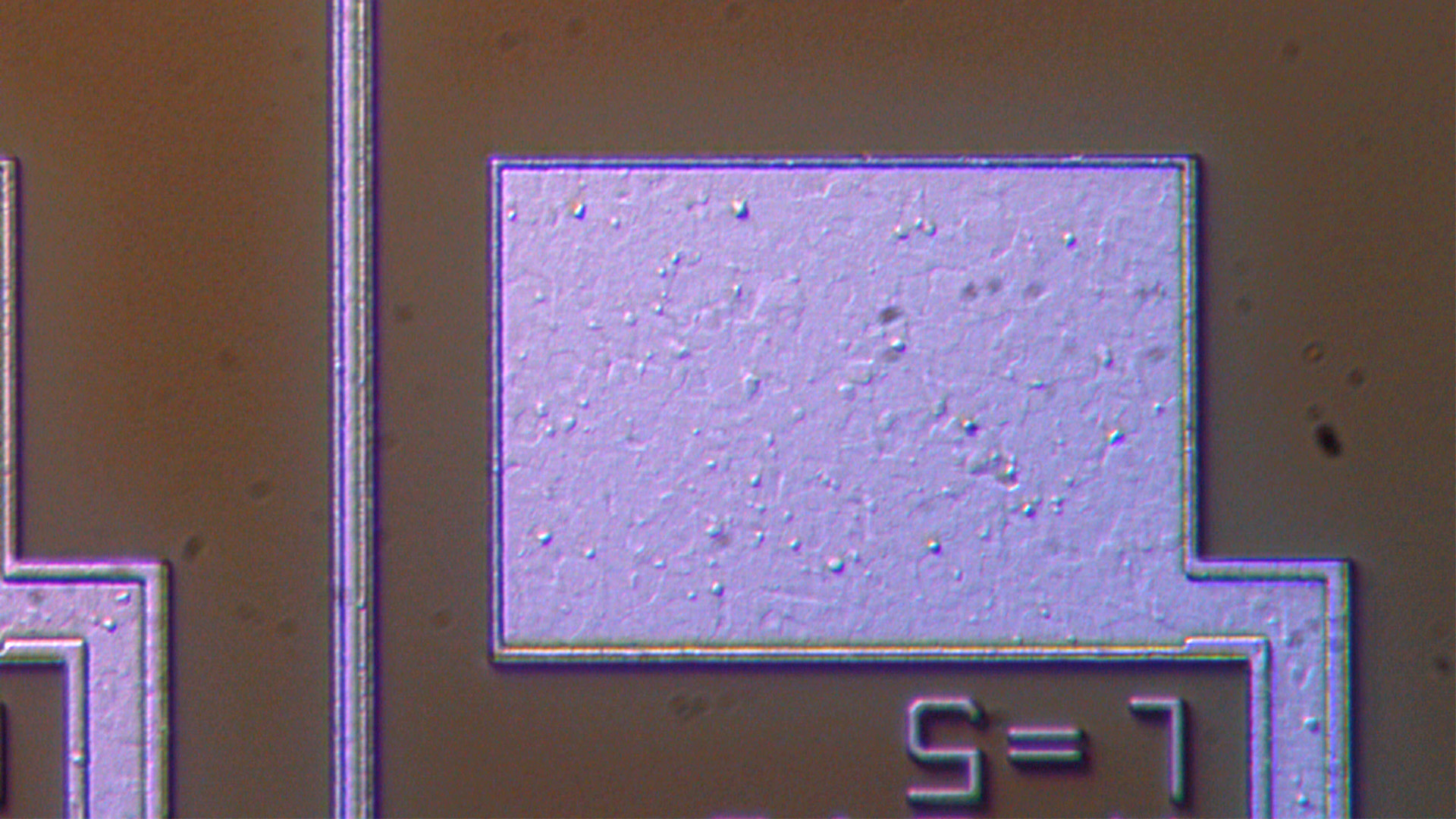
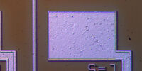
To achieve more efficient and reliable wafer inspection and quality control (QC), it is crucial to visualize difficult-to-see details easily. When using a microscope solution for inspection, the image quality, in terms of contrast and level of detail easily seen, depends strongly on the illumination and optics.
Choosing the appropriate illumination and contrast method, such as brightfield, darkfield, UV, and oblique illumination, can be imperative. Different wafer and IC-chip defects, e.g., contamination, residue, smeared coatings, scratches, etc., often can be more visible with one contrast method compared to others.
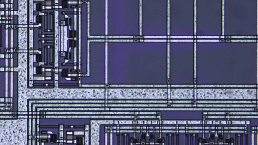
Cross-Section Preparation and Analysis
To examine the internal structure of semiconductor components, like IC chips, preparing and analyzing cross sections is necessary due to opaque materials. Cross-section analysis is a valuable method for inspection, along with failure analysis and R&D. It requires cutting through a semiconductor component then grinding and polishing the cross section to obtain a smooth surface.
Cross-section analysis can be performed with optical microscopy alone. If microscopy is combined with laser spectroscopy, then both the internal structure and composition of semiconductor components are revealed simultaneously.

Frequently Asked Questions Semiconductor Inspection
Semiconductor manufacturing is the process where integrated-circuit (IC) chips are produced. First, layers of conducting and insulating thin-films are deposited on a wafer made of semiconducting material like silicon (Si). Next, nanopatterns are formed by depositing a photoresist layer on top of the wafer, exposing it to UV light through a mask, and then etching of the exposed areas. After washing away the photoresist, the electrical conductivity of the patterns are tuned by ion bombardment and ICs are built. Finally, the patterned wafer is cut into IC chips which are then mounted onto a printed-circuit board (PCB).
Several processes and steps are required for semiconductor manufacturing to produce electronic components like IC (integrated-circuit) chips. It involves a range of nanofabrication processes and equipment like UV lithography, dry and wet etching, and ion beams. Because of the tiny dimensions of nanopatterns, dust and other contamination must be avoided, otherwise serious defects can result. For this reason, semiconductor manufacturing is done in a clean room. Inspection using optical microscopes and other techniques is an important part of the manufacturing. It is performed regularly to ensure few or no defects and high component quality.

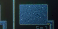
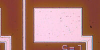
. With DIC users are able to visualize small height differences on the wafer surface more easily.")


 and oblique (right) brightfield illumination using a Leica compound microscope. The defect on the wafer surface is clearly more visible with oblique illumination.")
 chip cross section acquired at higher magnification showing a region of interest.")


