Contact Us

Thank you for your message

We will use the information you provide to process your request and to maintain a record of your request and our response. We will aim to complete your request as soon as reasonably practicable and consistent with any applicable laws.

A member of our Leica team will come back to you shortly with the information you requested.

Your input is valuable for us and we want to take time to answer each message carefully. Please be assured that Leica Microsystems and its agents will use your contact information for the purposes of business communication with you. We will not sell this information for advertisement or to third parties.

Your Options

Latest articles

Particulate contamination in between moving metal plates.

Key Factors for Efficient Cleanliness Analysis

An overview of the key factors necessary for technical cleanliness and efficient cleanliness analysis concerning automotive and electronics manufacturing and production is provided in this article.
Microscope equipped with a K7 color CMOS camera for life-science and industry imaging applications.

Technical Terms for Digital Microscope Cameras and Image Analysis

Learn more about the basic principles behind digital microscope camera technologies, how digital cameras work, and take advantage of a reference list of technical terms from this article.
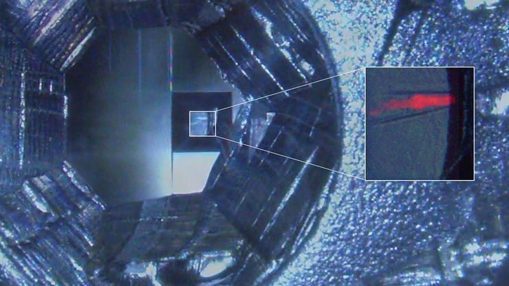
Images of the same area of a processed wafer taken with standard (left) and oblique (right) brightfield illumination using a Leica compound microscope. The defect on the wafer surface is clearly more visible with oblique illumination.

Rapid Semiconductor Inspection with Microscope Contrast Methods

Semiconductor inspection for QC of materials like wafers can be challenging. Microscope solutions that offer several contrast methods enable fast and reliable defect detection and efficient workflows.
Preparation of an IC-chip cross section: grinding and polishing of the chip cross section.

Cross-section Analysis for Electronics Manufacturing

This article describes cross-section analysis for electronics concerning quality control and failure analysis of printed circuit boards (PCBs) and assemblies (PCBAs), integrated circuits (ICs), etc.

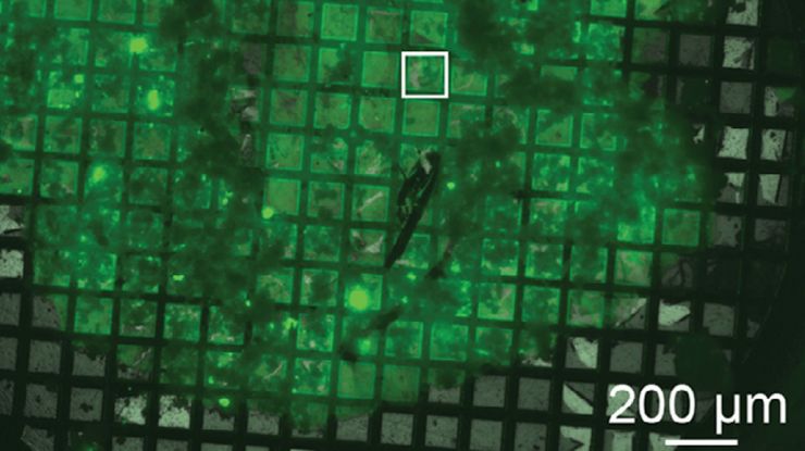
Studying Virus Replication with Fluorescence Microscopy

The results from research on SARS-CoV-2 virus replication kinetics, adaption capabilities, and cytopathology in Vero E6 cells, done with the help of fluorescence microscopy, are described in this…
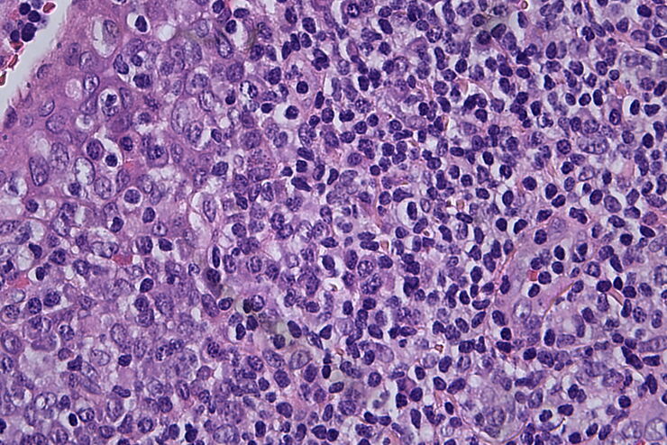
Fluorescence microscopy image of liver tissue where DNA in the nuclei are stained with Feulgen-pararosanilin and visualized with transmitted green light.

Epi-Illumination Fluorescence and Reflection-Contrast Microscopy

This article discusses the development of epi-illumination and reflection contrast for fluorescence microscopy concerning life-science applications. Much was done by the Ploem research group…
Material sample with a large height, size, and weight being observed with an inverted microscope.

Five Inverted-Microscope Advantages for Industrial Applications

With inverted microscopes, you look at samples from below since their optics are placed under the sample, with upright microscopes you look at samples from above. Traditionally, inverted microscopes…

Coherent Raman Scattering Microscopy Publication List

CRS (Coherent Raman Scattering) microscopy is an umbrella term for label-free methods that image biological structures by exploiting the characteristic, intrinsic vibrational contrast of their…
Image of an onion flake taken with a basic Leica compound microscope after it was tested for resistance to fungus and mold growth following part 11 of the ISO 9022 standard.

ISO 9022 Standard Part 11 - Testing Microscopes with Severe Conditions

This article describes a test to determine the robustness of Leica microscopes to mold and fungus growth. The test follows the specifications of the ISO 9022 part 11 standard for optical instruments.
Scroll to top