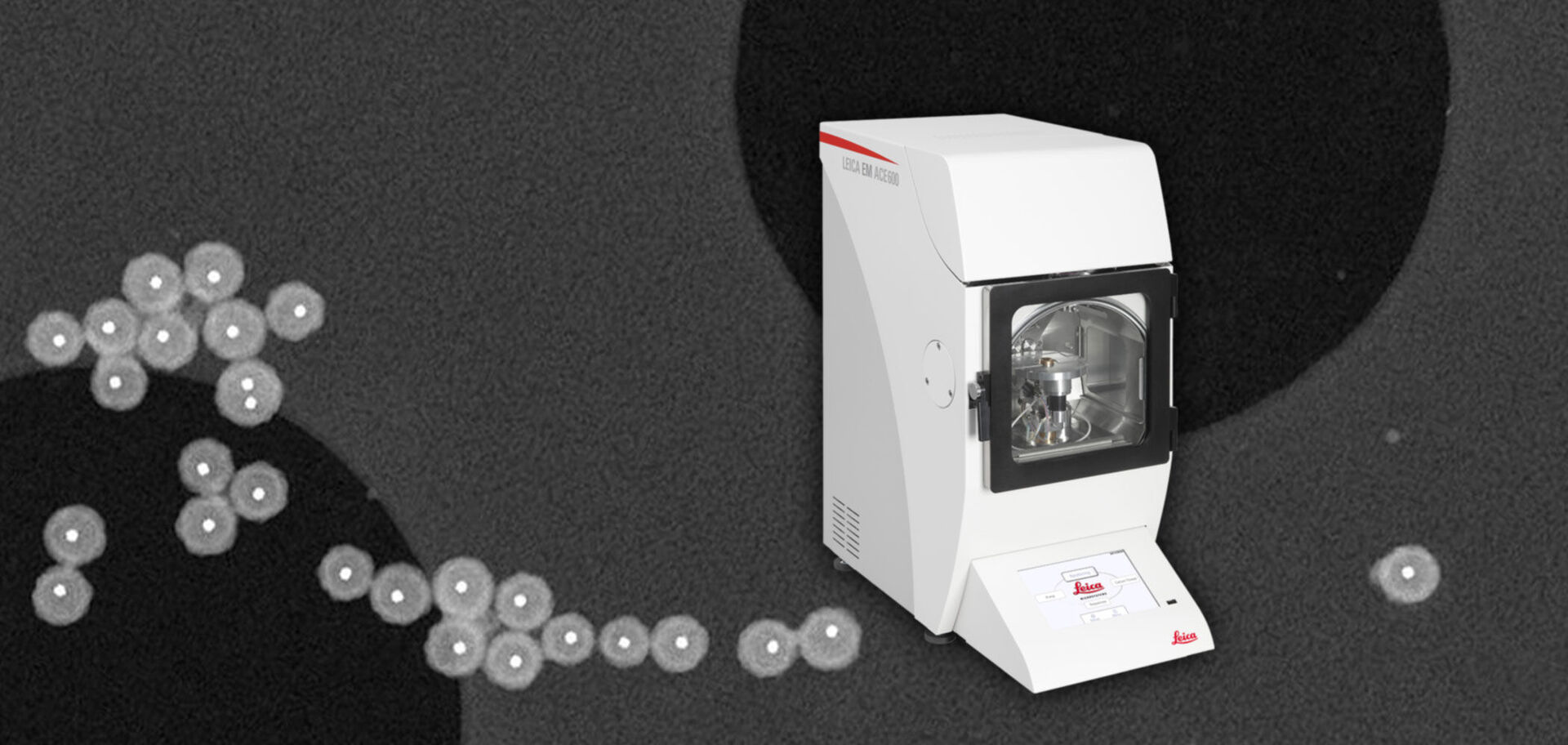
EM ACE600 Sputter Coater
Prepare with confidence the fine grained thin films you need for electron microscopy analysis with the EM ACE600 sputter coater. Precise, automated carbon and sputter coating processes yield reproducible results you can trust and enable you to increase your sample output with every run.
High Vacuum Coating System for a wide range of applications
Equipped with a configurable metal process chamber, the EM ACE600 sputter coater is flexible and can be adapted to a wide range of applications. Reach your workflow goals and meet the needs of your lab by running up to two different sources in a single preparation process or even configure the EM ACE600 for advanced cryo workflows.
The EM ACE600 makes your routine sample preparation simple and reliable and saves valuable time with the convenience of front door loading, automated, and receipt-based coating processes which can be started by a single button press.
Whether you need to…
- Perform high-resolution imaging of flat or structured non-conductive specimens
- Enhance the contrast of nanometer scale structures, such as proteins or DNA strands
- Produce thin, but strong support layers for TEM grids or
- Provide protection layers for sensitive samples
- Expand the system for cryo applications
… with the EM ACE600 carbon and sputter coater you got it covered.

Reproducible high-quality thin films with sputter coating
Produce high-quality, sputter coated thin films consistently with every run with the EM ACE600 high vacuum coating system. Meet the right conditions for your advanced coating needs and achieve reproducible results thanks to the automated, receipt-based sputter coating process.
Perform high magnification SEM analysis up to 200kX and beyond, with an excellent base vacuum of <2x10⁻⁶ mbar and fine balanced process parameters for a range of sputter targets. Adjust the sample distance and coating angle to the needs of the morphology of the sample.
To even further enhance your coating results, you can use a Meissner trap to increase the vacuum to 10-7 mbar regime, and then try sputter targets or sample materials which are sensitive to oxygen.

Reproducible, high-quality thin films with carbon coating
With the EM ACE600 you can produce high-quality carbon films by using carbon thread coating, carbon rod coating, or e-beam evaporation.
Carbon thread evaporation has become a widely used method since
Leica Microsystems developed the unique adaptive pulsing approach implemented into the EM ACE600. It can produce precise, robust, and amorphous films with sub-nanometer thickness while minimizing the heat impact on the sample. Whether you are in need of nanometer thin, strong, and clean TEM support layers, diffuse (protection) coatings, or large homogeneous carbon layers, carbon thread is right choice.
For dedicated applications, such as rotary shadowing, you can use the e-beam evaporator. Its small beam divergence is ideal for shadow coating to enhance edge contrast of nanometer scale structures.

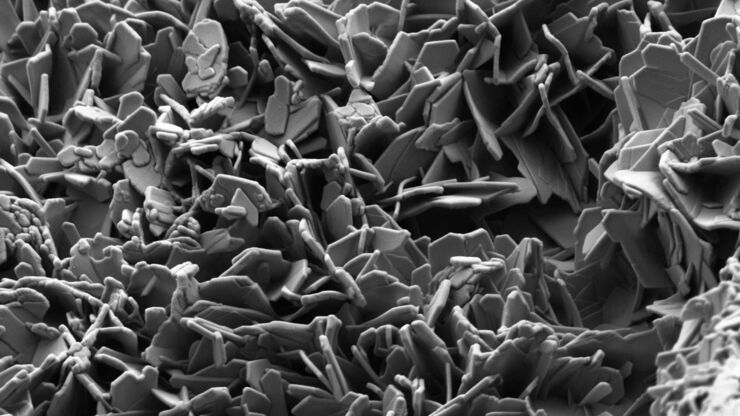
Ultra thin carbon films
Carbon coating has multiple applications for electron microscopy. It needs to be conductive, but invisible for the electron beam and should not have grain structure.
Thin films produced by the EM ACE600 carbon thread with adaptive pulsing are precise in thickness, strong, conductive and can even be baked out for further reduction of contamination. Ultimately, such films provide:
- High transparency to electrons
- Adequate strength to withstand electron bombardment
- Uniform thickness, crucial for analytical investigations, quantitative imaging, or electron tomography

Adapt the EM ACE600 to your needs
Run more than one process in a single coater instrument without breaking the vacuum, thanks to the large configurable metal process chamber of the EM ACE600. Simultaneously, combine a sputter head with an advanced carbon thread evaporator or choose two sputter sources enabling multi-layer metal coatings in a single preparation process.
- Produce evenly distributed thin films over the entire 100 mm stage thanks to the optimized two-source concept with two angled ports and a rotating stage
- Choose from robust carbon thread, e-beam, and sputter coater sources
- Equip your EM ACE600 with glow discharge sputtering
- Upgradable at any time on site

Stay focussed on the critical parts of your preparation process
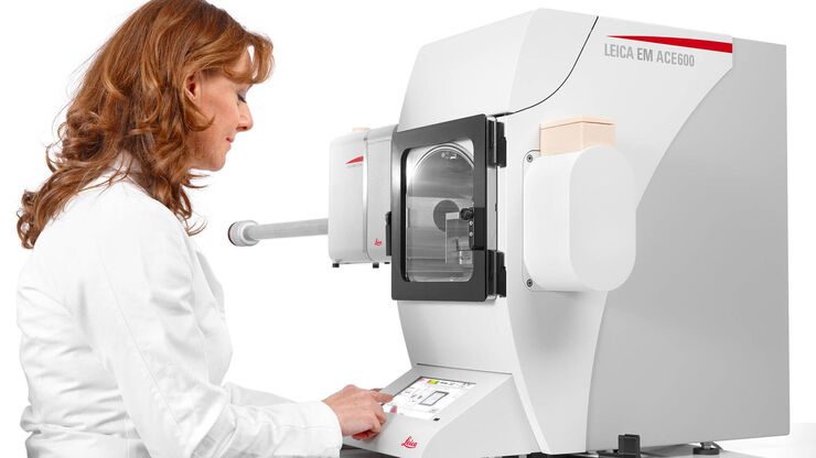
Be confident that your routine sample preparation gets done with the press of a single button by using the EM ACE600 carbon and sputter coater. Simple and reliable workflows and convenient standard operating procedures enable you to focus on the critical parts of EM sample preparation. You can concentrate on optimizing your workflow and spend less time learning how to operate the system or training others how to use it.
- Safe loading and unloading of sensitive samples via the front door
- A workflow-based user interface and fast access to relevant parameters guides the way
- Light-weight and robust sources for convenient daily handling

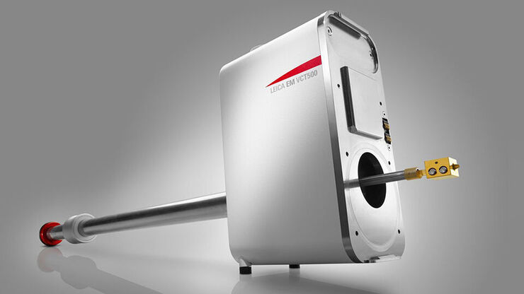

Expand to Cryo Workflows
Open up your laboratory to a full range of electron microscopy experiments by coating your samples under cryo conditions. The EM ACE600 carbon and sputter coater supports sample preparation for research, like structural analysis of biological samples in their native and hydrated state, by performing freeze fracture and, cryo coating followed by cryo sample transfer into the SEM with the help of the EM VCT500 transfer system.
The EM ACE600 offers:
- An interface for cryo sample transfer
- A cryo stage for coating under cryogenic conditions
- A basic fracture device

Choose the optimal configuration
Meet the needs of your daily lab work by configuring your EM ACE600 carbon and sputter coater.
Choose from a broad selection of sample holders and stages such the 3 axis stage with up to 3 motorized axes or the dedicated cooling stage. Quickly exchangeable stage dishes make your EM ACE600 a multi-purpose tool.

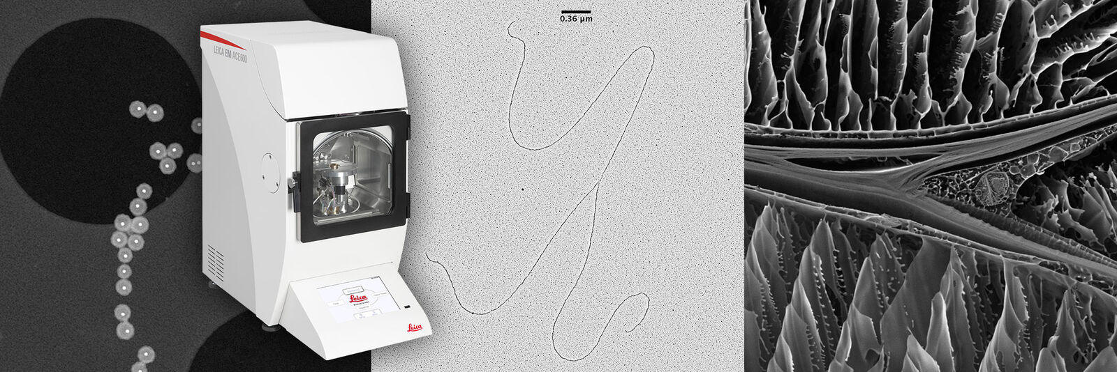
Rotary Shadowing – make nanoscale structures visible
Configure your EM ACE600 with a dedicated low angle rotary shadowing (LARS) setup so you can image nanometer scaled structures, such as proteins or DNA strands, in the TEM. The EM ACE600 e-beam source together with a motorized LARS stage combines directive, low heat – impact, thin - film deposition with an optimized stage geometry for grazing incidence deposition. Once the DNA strands are shadow coated at a small angle with a fine grained platinum layer, a carbon layer is added to stabilize the fragile structures for analysis in the TEM.

Choose the right workflow for your experiment
The EM ACE600 helps you get high quality results when conducting material science and biological experiments.
Workflows range from standard TEM and SEM sample preparation to section tomography 3D workflows, FIB SEM, and more. For more information on workflow solutions for
- life science research, download workflow booklet
- material science research, download workflow booklet
Standard SEM Workflow
Investigate the surface architecture of chemically fixed samples with the standard SEM workflow. Prepare your samples with the EM TP tissue processer and critical point dry them afterwards with the EM CPD300. The next step is coating your samples with either the EM ACE200 or EM ACE600 followed by imaging in the SEM.

SEM / LM Solid State Preparation - Broad Ion Beam Cross Sectioning
This technique is most commonly used for solid state SEM samples, but can be applied for LM investigations as well. When the sample has a certain target to be exposed for observation, the sample needs to be well-cut to get the inner structure of the part of interest. Afterwards, for non-conductive samples, coating is necessary to make the sample suitable for SEM observation.

Cryo-SEM Sample Preparation and Transfer - Broad Ion Beam Cross Sectioning
This cryo transfer workflow is used for high pressure frozen samples including hard and brittle material (e.g. clay with quartz). The sample has to be kept at a temperature -150 °C during the complete preparation process, from high pressure freezing, over mechanical pre-preparation using the cryo-saw, followed by an ion beam milling step and finally transferring it to the Cryo-SEM.

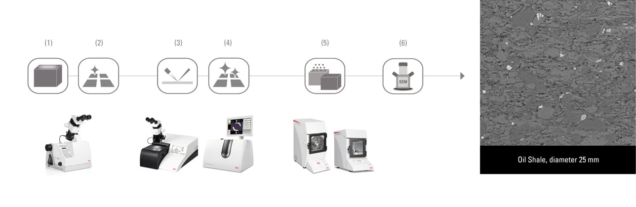
SEM / LM Solid State Preparation - Broad Ion Beam Polishing
This technique is used for large solid state SEM or LM samples. When a large area (several cm2) of the sample has to be investigated at a highest quality level (e.g. EBSD), the sample is mechanically pre-prepared (mirror-like finish) and finally prepared with the ion beam polishing method.
Section Tomography 3D Workflow
With this workflow you can study the organization and interaction of biological structures within a defined 3D volume. The first step is to process your samples at room temperature, followed by semi-thick serial sectioning onto TEM grids. After the staining step, then proceed with TEM imaging.

