
Introduction to broad ion beam milling
Broad ion beam milling utilizes ionized argon gas to bombard the sample, and physically sputter atoms from the sample. When done in cross section (also known as slope cutting), as demonstrated here, a carbide mask is positioned between the ion beam and the sample, which serves to define the position of the cross-section surface, as well as protect the front surface of the sample. When done properly, the slope cutting process results in a pristine cross section, regardless of sample material properties or composition.
Step by step preparation of lithium batteries for electron microscopy analysis
In this application note, a combination of mechanical preparation and broad ion beam milling are used to prepare two components of a battery system – a lithium nickel manganese cobalt oxide/aluminum (Li-NMC/Al) electrode and a lead (Pb) grid. For both samples, the mechanical preparation and ion milling followed a similar protocol. Mechanical preparation was carried out using the Leica Microsystems EM TXP target surfacing system, which is a highly precise benchtop tool that can be used to saw, grind, polish, and mill samples with in-situ sample observation. Ion milling was carried out on the Leica EM TIC3X broad ion beam milling system, to achieve the final pristine cross section.
Preparation protocol
Both samples, the Li-MNC and the Pb grid sample have been mounted between glass slides using 2-part epoxy, then fixed to the Leica TIC3X sample holders prior to preparing on the TXP. Fixing the sample between glass slides provides additional support for the sample, while avoiding the need to fully embed in other mounting materials such as epoxy. This also reduces the surface area for the grinding and polishing processes and allows the sample to be mounted on a single sample holder for the entirety of the workflow.
a) Mechanical Preparation
The samples were then mounted on the TXP chuck and ground on the TXP down to a 9 μm finish using diamond lapping foils. The sample was then tilted to a 60° angle, and a bevel was ground into the front-facing glass slide using 400 grit silicon carbide sandpaper. This removes excess glass from the cross-section surface, reducing the amount of material to be displaced by the ion mill, therefore speeding up the ion milling process and increasing throughput. Preparation time was approximately 20 minutes.
b) Milling with the triple ion beam milling system
The sample holder was then mounted directly onto the TIC3X adapter for ion milling in the standard stage for room temperature slope cutting. Each sample was milled at 8 kV. The milling time was 3 hours for the Li-MNC electrode and 6 hours for the Pb grid. The disparity in milling time is due to the difference in sample dimensions.
SEM analysis
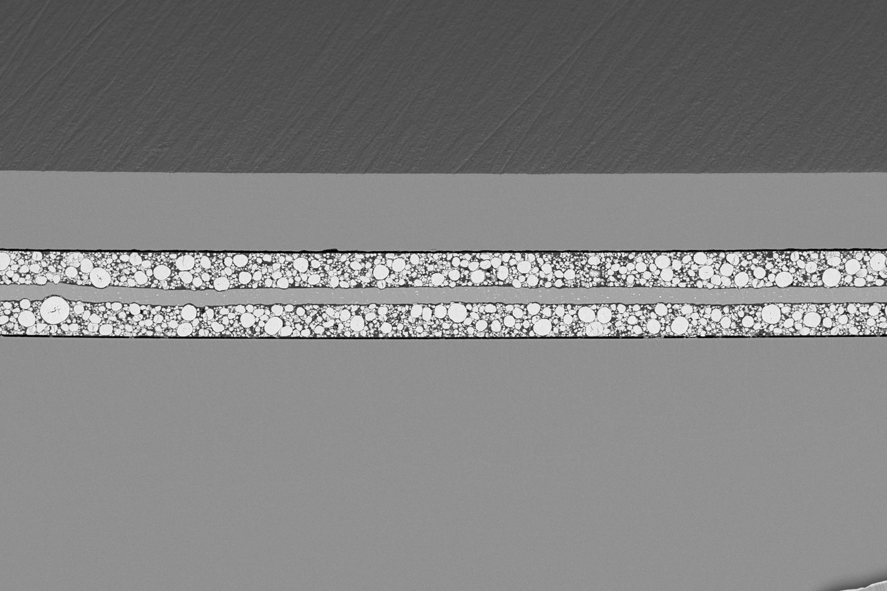
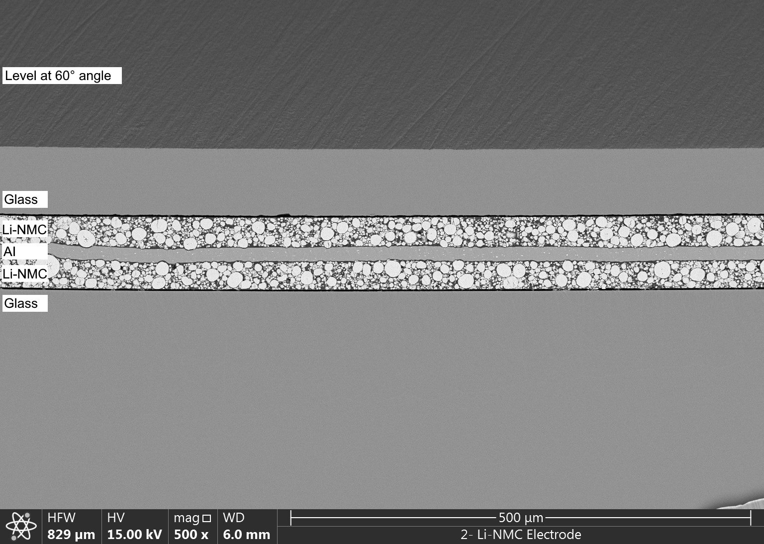
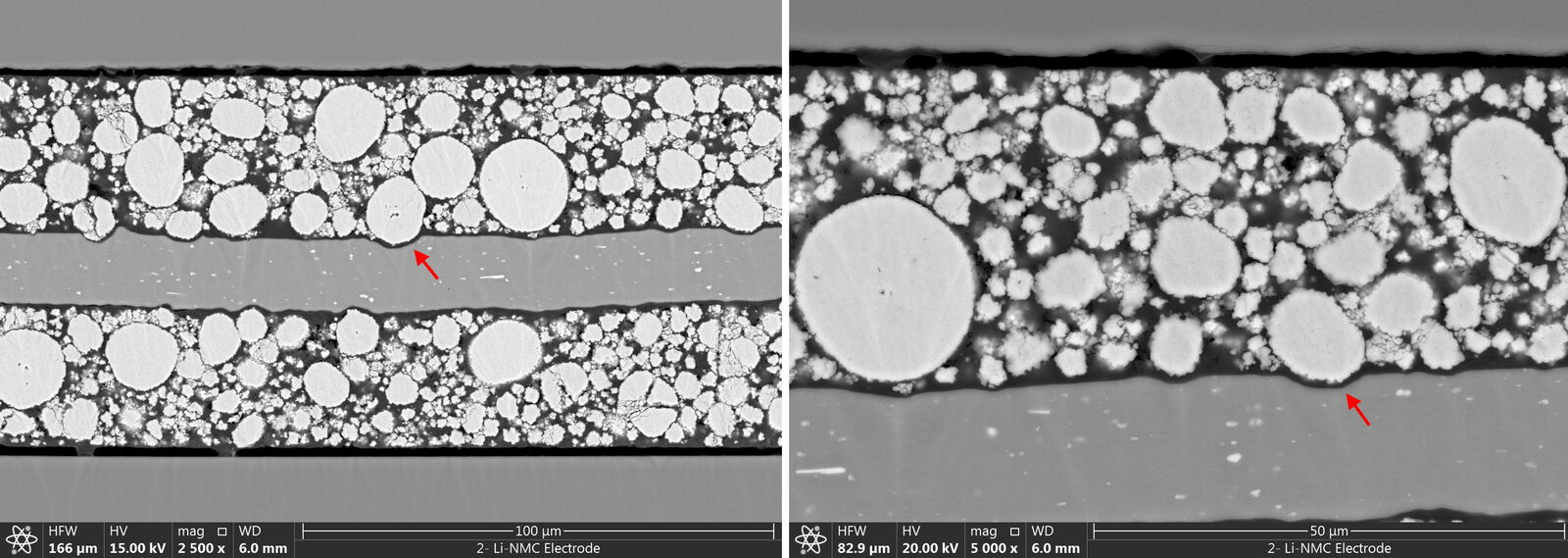
Figures 1 and 2 show SEM images of the Li-MNC electrode sample. Figure 1 shows the full stack of all layers in this sample, including the two pieces of glass used to mount the sample and the oxide/metal sandwich structure of the electrode. Figure 2 shows higher magnification images focusing on the sample material of interest. From these images, the high quality of the preparation can be observed in the smooth defect-free surface on the sample. These results can be used to determine particle size and distribution within the electrode material. Additionally, accurate thickness determination can be made for the full electrode sample as well as individual layers. Also of interest is the interface between the porous films and the metal film at the center of the structure. The images show how the metal film conforms to the grains of the porous layers (indicated by the red arrows) and if there was delamination within the structure, that should be visible in these images as well.
Microscopy techniques suited to image multicolor reporter lines
Figure 3 shows SEM images of the Pb grid sample. From these images, the high quality of the cross section can be observed. The surface of the sample is pristine and the grain structure of the Pb grid is clearly visible, without any additional etching. From this sample, it is possible to analyze grain size and orientation, and while not captured on this sample, this processing quality is generally suitable for electron backscatter diffraction (EBSD) analysis. In these images, we can clearly see regions where grain size varies significantly – there are regions where the grains are fairly coarse and other regions where the grain structure is very fine. The grain boundaries are also easily visible.

Samples provided courtesy of East Penn Manufacturing Co. Sample preparation and images courtesy of Jerome Pons, JH Technologies.
 at the edge of a battery electrode acquired with a DVM6 digital microscope.")


