
The ion beam etching method
Ion Beam Etching, also known as Ion Beam Milling or Ion Milling, is the most widely-used etching method for preparing solid state samples for scanning electron microscopy (SEM) applications. In this process, the sample material is bombarded with high-energy argon ion beams in a high vacuum chamber. The top layer of the material is removed by high energy ions to achieve a defect-free sample surface. The ion energy and milling angle depend on the corresponding application and can be adjusted accordingly. It is also possible to improve the quality of mechanically polished surfaces via a final ion polishing process. The surfaces of samples can be cleaned, polished and have their contrast enhanced using ion milling techniques. These techniques are used to obtain high resolution SEM images for various applications such as failure analysis and to perform surface sensitive analyses such as EBSD for material characterization.
Cutting and Polishing
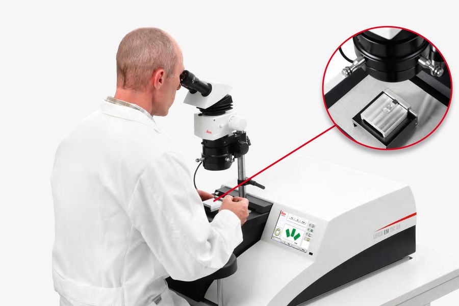
Preparation often begins with a need to accurately cut, grind and polish the surface prior to ion beam milling and metal/carbon coating. With the Leica EM TXP target preparation system all required machining steps can be completed in one instrument – from diamond cutting and milling to polishing.
High quality surfacing
The unique broad ion beam milling system of the Leica EM TIC 3X is the system of choice for EDS, WDS, Auger and EBSD, because ion beam milling is often found to be the only method capable of achieving high quality cross-sections and planed surfaces of almost any material. The process reveals the internal structures of a sample whilst minimizing deformation or damage.
EM TIC 3X Ion Beam Milling Machine
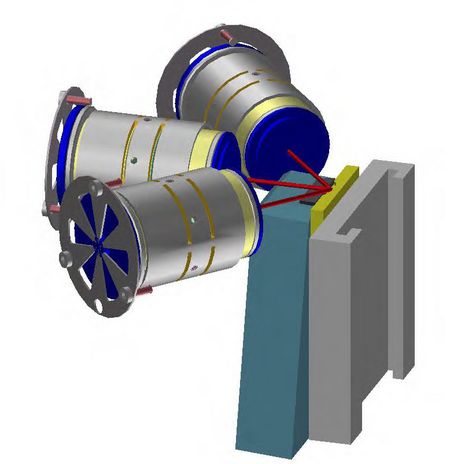
The EM TIC 3X is a broad ion beam milling unit that is used to prepare sample cross sections as well as planar samples for scanning electron microscopy (SEM), light microscopy (LM), microstructure analysis (EDS, WDS, Auger, EBSD) and atomic force microscopy (AFM) investigations. The instrument is equipped with a triple ion beam system and can process large surface areas of almost any material at room temperature or cryo.
The EM TIC 3X is setup as a modular system and can be flexibly equipped with different stages for various applications
- Standard stage: prepare a wide range of samples with different sizes, shapes and materials
- Cooling stage: prevents thermally-cooling sensitive samples from being destroyed by overheating
- Multiple sample stage: prepare at least three samples successively without user interaction guaranteeing a high-level sample throughput.
- Rotary stage: for flat milling or ion beam polishing
Cross section sample preparation by ion beam etching
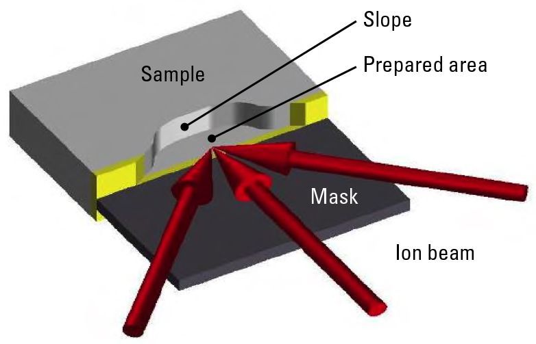
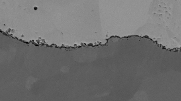
Ion beam slope cutting is a method for producing sample cross-sections for scanning electron microscopy (SEM). This method has its origins in an idea from Wolfgang Hauffe, who initially used this method only for producing diagonal cuts. This is what led to this method being referred to as slope cutting.
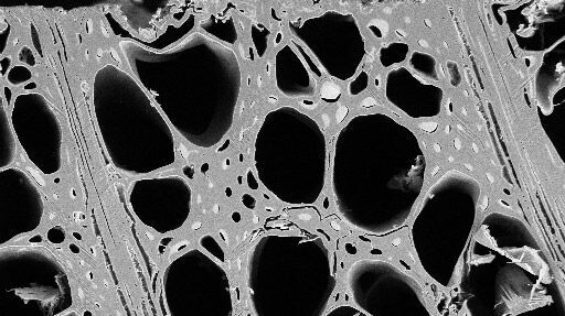
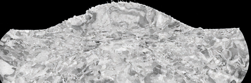
To produce cross sections for scanning electron microscopy (SEM), the sample is covered with a sharp-edged mask such that only 50–100 µm of the sample material is exposed above the mask. The three ion beams intersect at the center of the mask edge and strike the uncovered material and remove it to produce a sample cross-section with a high surface quality. The design of the ion gun develops a milling rate of 300 μm/hour (Si 10 kV, 3.5 mA, 100 μm from edge). This unique technique produces a vast cross sectioning area of larger than 4 × 1 mm at a high material removal rate to achieve a high-quality surface finish.

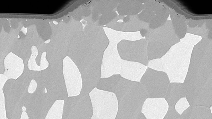
Planar sample preparation by ion beam etching
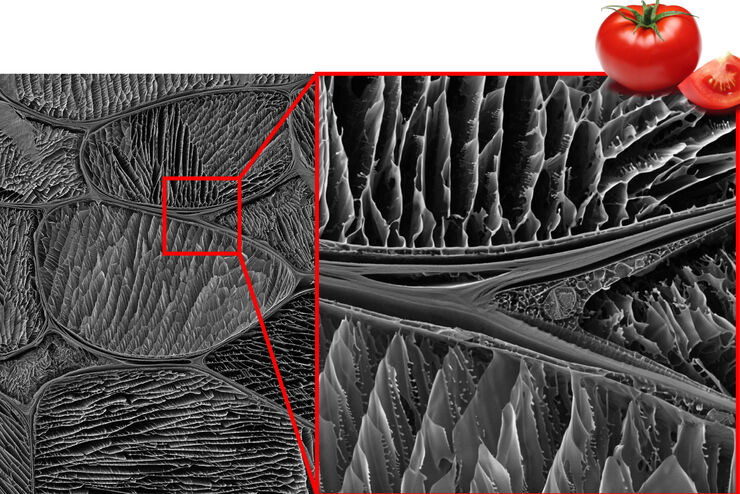
For flat milling (or ion beam polishing) the rotary stage is used. Due to the gun assembly and additional lateral movement of the sample, a uniform, high quality area larger than 25 mm diameter can be prepared. This preparation process is used to clean, polish or enhance the contrast of a mechanically or chemically polished surface with the goal of removing fine scratches, abrasive material and smearing artifacts.

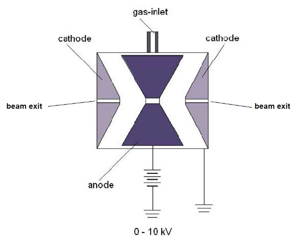
The working principles of the EM TIC 3X unique triple ion beam system
The triple ion source of the EM TIC 3X consists of three independent controllable saddle-field ion guns. The ion energy is adjustable between 1 to 10 keV. The ion source will be fed with a process gas, preferably Argon. A high voltage (1 to 10 kV) will be applied on the anode. The cathodes and Wehnelt cylinders are on earth potential. Due to the electrical field between anode and cathode the process gas will be ionized (Ar+) and the plasma ignites. Positive charged ions will be accelerated towards the cathodes and generate electrons. This bombardment leads to an abrasion of the cathode. Negative charged electrons will be accelerated towards the anode and collide with gas atoms and generate ions. Due to the shape of the electrical field between anode and Wehnelt cylinders (saddle field) two ion beams are created and accelerated towards both cathodes. One beam is blocked by the (blind) rear side cathode. The other beam will be led through the beam exit at the front side cathode. The energy of the ions coming out matches the acceleration voltage.
Related articles
Application Booklet for EM TIC 3X

Workflow Solutions for Sample Preparation Methods for Material Science
Practical Applications of Broad Ion Beam Milling
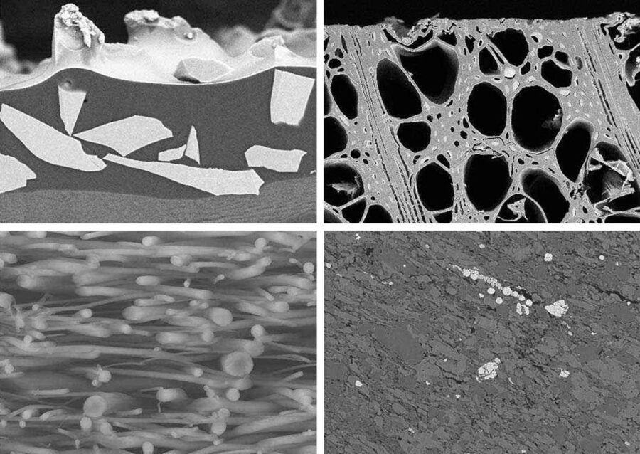
Cleaning sample surfaces and contrast enhancement
For better showcasing the grain structure in polycrystalline materials, a chemical etching process where the individual grains are etched to varying degrees is normally used. This results in topography that enhances contrast.
This contrast enhancement, however, can also be generated by ion milling. Milling angles in a range of 30° to 90° are used in relation to the sample surface in this process. The angle depends on the material being prepared and its milling rate. The ion etching process, unlike conventional chemical etching, has a number of advantages. It is cleaner, safer and, above all, can be controlled better.
Enhanced Resolution with Ion Beam Milling
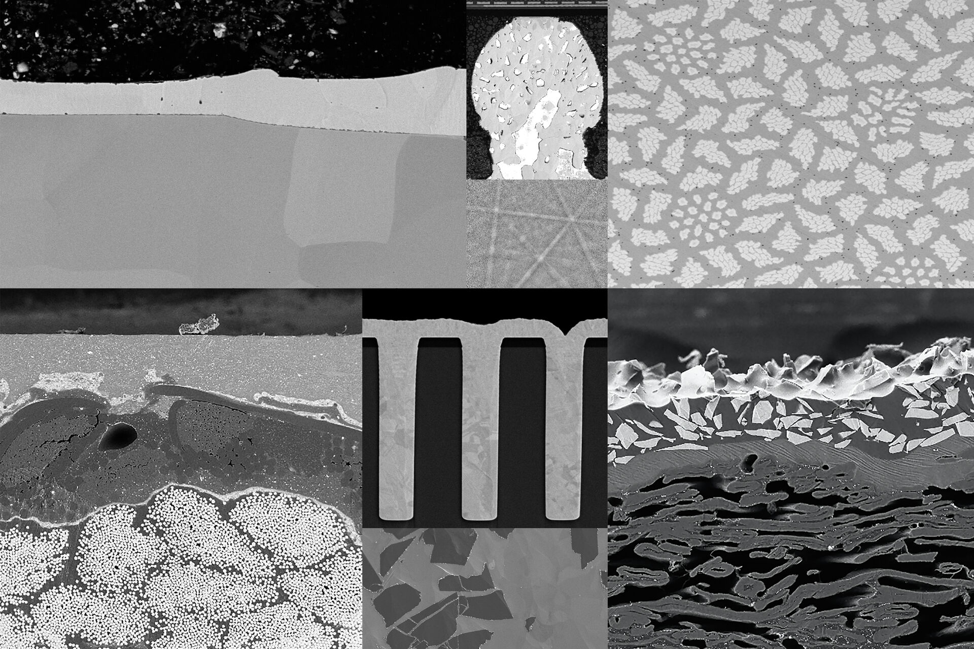
The Ion Beam Milling technique, also known as Ion Beam Etching, is used to achieve a well-prepared sample surface quality for high resolution imaging and analysis. It removes residual artefacts from mechanical cutting and polishing. The ion polished cross-sections and planar samples prepared by Ion Beam Etching can be used for electron microscopy imaging as well as microstructural analysis applications such as EDS, WDS, Auger and EBSD.
The EM TIC 3X Milling Machine offers triple ion beams that speed up the preparation process significantly and achieve to reveal finest details and structures on sample surfaces. Watch the video and see how to cut the preparation time for IC gold wire bonding using the Target Surfacing System EM TXP and the EM TIC 3X Ion Beam Milling System.
Sample Preparation for EBSD
EBSD is a surface sensitive examination method with an information depth of just a few nanometers. For sample preparation, this results in very high requirements. The sample surface should be very smooth and free of damage of any kind. These requirements can be met using two different methods of ion beam preparation: ion beam slope cutting and ion beam polishing. Prepared areas of no more than 8 mm in length and 1–2 mm in depth are achieved during ion beam slope cutting. Mechanical pre-preparation is necessary only for samples with an irregular shape or in the event of site-specific preparation. Ion beam polishing, on the other hand, requires perfect mechanical pre-preparation.
Leica EM TIC 3X
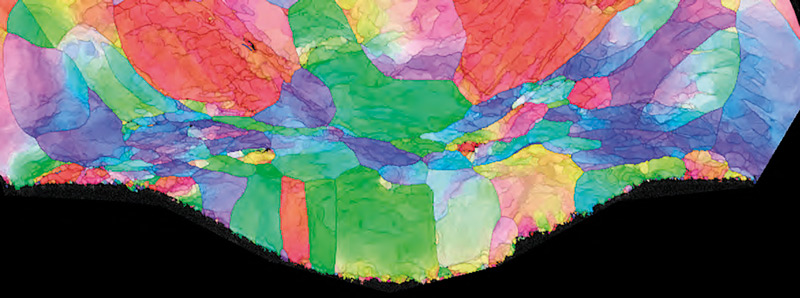
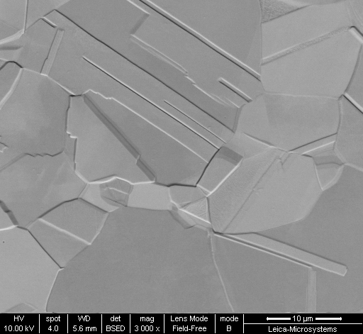
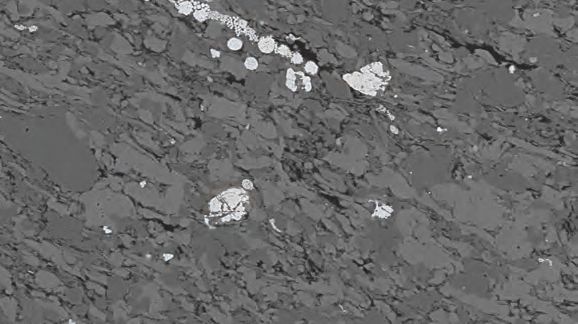
Au layers. Very fine deformation structures in the Au layer (of less than 40 nm) are revealed by the EBSD analysis. Courtesy of: Bruker Nano GmbH
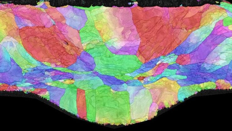
. The grains are highlighted with arbitrary colors.")


. The grains are highlighted with arbitrary colors.")


