DC magnetron method
Leica Microsystems developed a sputter coater which is based on the DC magnetron method – the Leica EM ACE600 device. A schematic of the principle is shown in Figure 1. Argon ions are accelerated towards the target materials by an applied electric field. This accelerated projectile generates neutral target atoms which fall down on the sample to form a thin conductive film. Besides the ejection of target atoms, secondary electrons are emitted by the impinged argon ions. These electrons are trapped inside a region near the target surface due to the additional annular magnetic field. The trapping of these electrons is the big advantage of this method. The electrons are forced to move along a circular path. This causes a drastic enhancement of the way inside the gas and leads to an increase deposition rate of the target atoms by using a much lower argon pressure.
Another advantage is that the local temperature increase on the sample is less than for other sputter coaters because the electrons which heat up the sample when they impinge on the surface are trapped in the magnetic trap near the target surface.
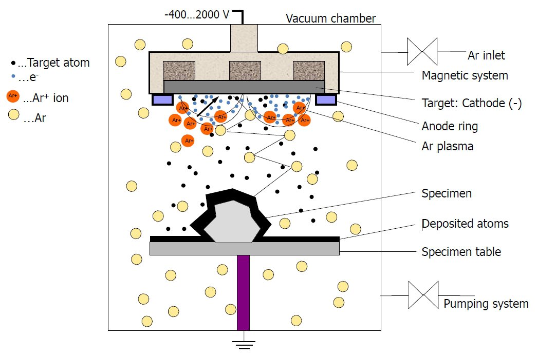
Fig. 1: Schematic of DC magnetron sputter coater
Film growth
Till an even film can be formed, there are several growth stages, which are depicted in Figure 2. One of the first stages is called nucleation. In this process grains are formed. Grains are clusters of atoms. Afterwards the grains grow further till they reach a critical radius. In a next step these grains minimise their surface by forming clusters, now called islands. Due to the minimisation of the surface area, channels and holes occur which have to be filled before the even film can be formed. Atoms inside the holes form again grains which fill these holes (secondary nucleation). All these effects are mainly based on the mobility of atoms on the surface and this diffusion is mathematically described by the surface diffusion [2]. Equation 1 shows the expression for the lateral surface diffusion D [m²/s] which depends on the lattice constant a [m], the amplitude of the diffusion frequency v0 [1/s], the diffusion energy ED [eV], and on the temperature of the sample TS [K].
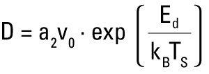
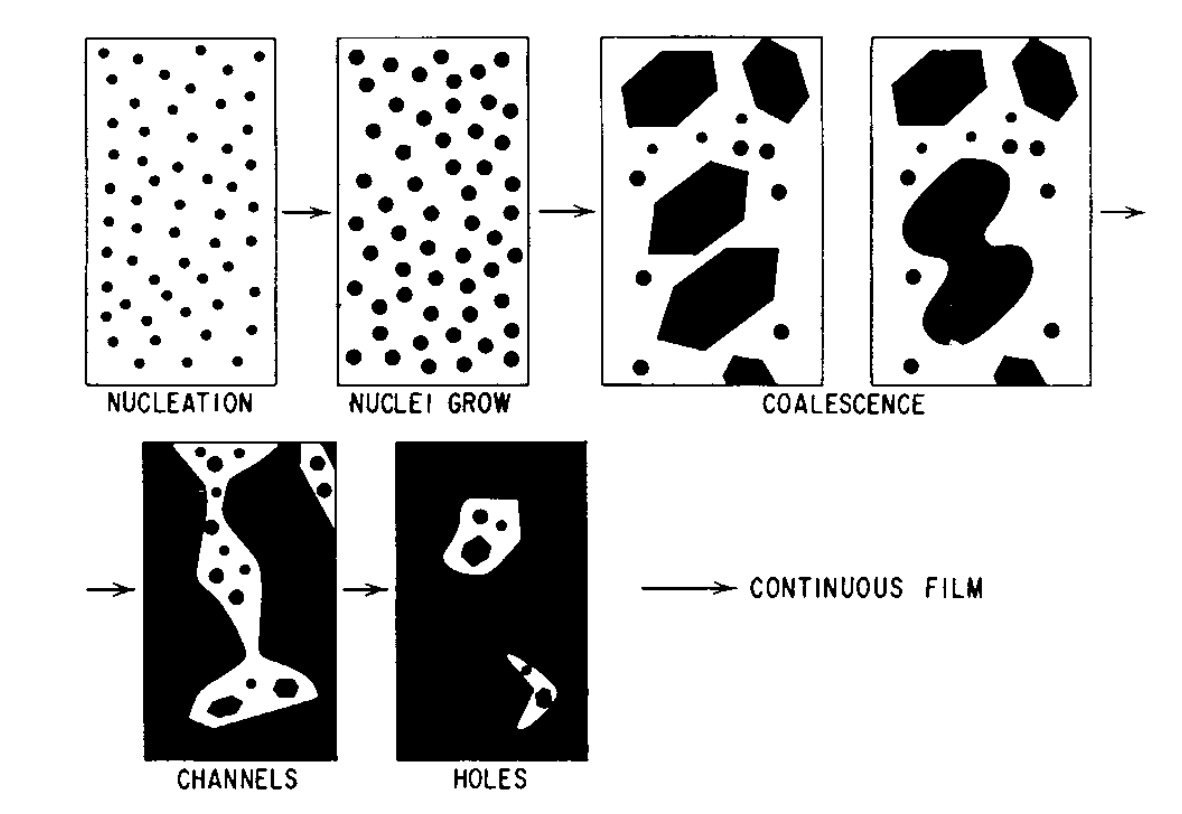
Fig. 2: Different growth stages [1]
Challenges and improvements
The resolutions of high end SEMs drastically increased during the last years, what leads to new upcoming problems. One of them is that previously used preparation methods are at their limits. The conductive layer has to fulfil more requirements at high magnifications than for magnifications which are used for investigations by using conventional SEMs.
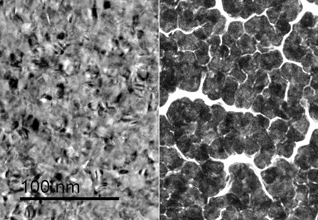
An example of a thin gold palladium film is shown in Figure 3.
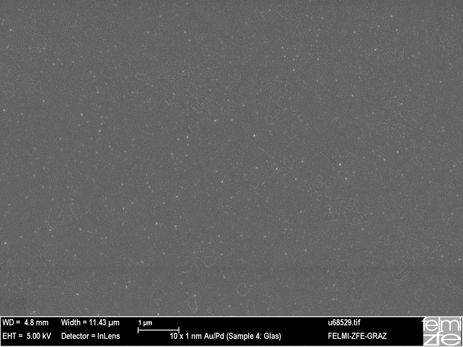
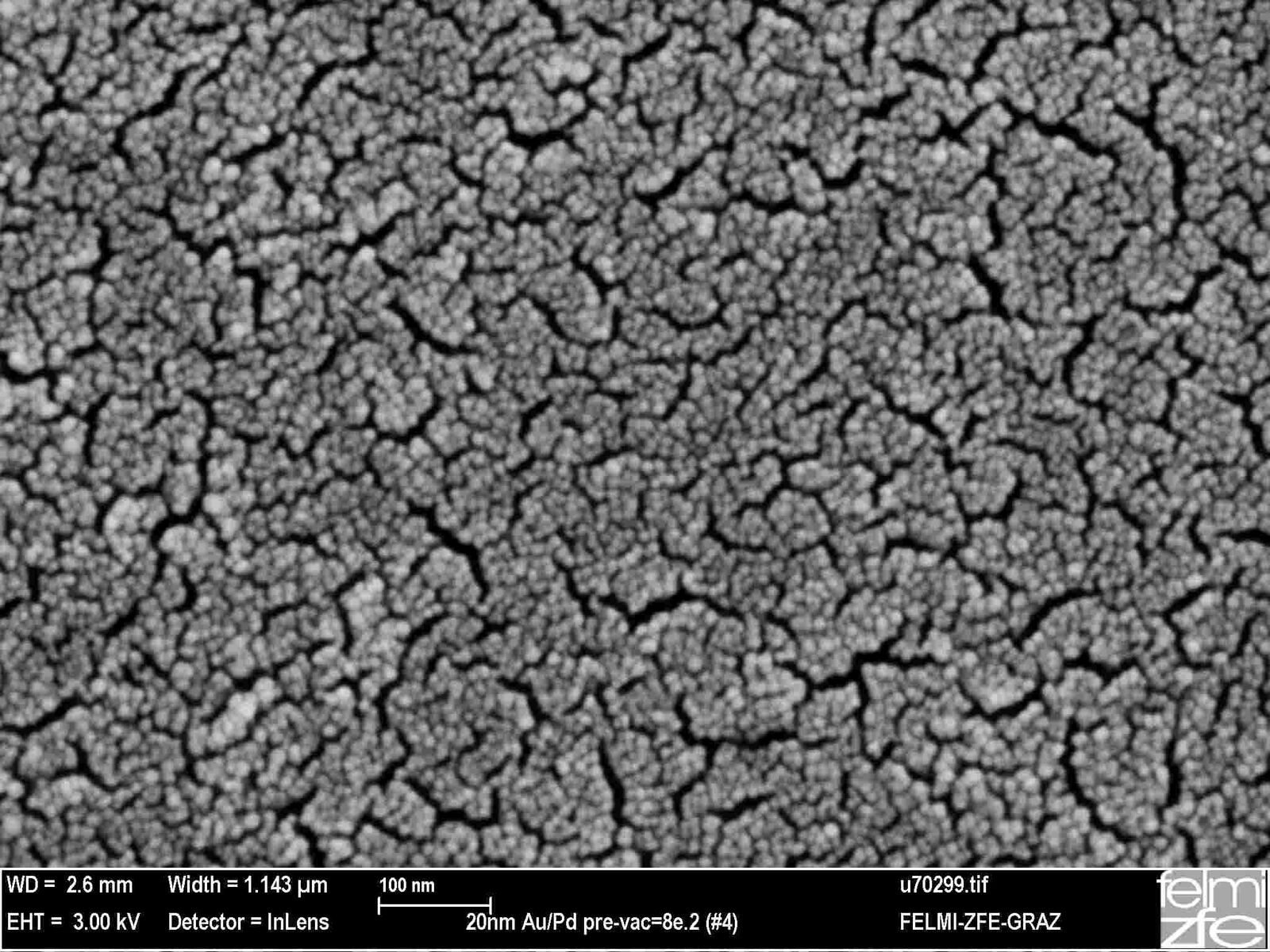
Fig. 3: Comparison between a thin film which is observed by low magnification (left) and by high magnification (right).
At high magnification thin films show a structured surface which is not applicable for high resolution. The ditches which can be seen in Figure 3 (right) leads to a higher surface resistivity. This causes drifts and charging effects during image acquisition by high magnification. Therefore the morphology of thin films has to be improved for using it.
Characterisation of the device
Before the sputter coater is optimised for high resolution applications, the verification of the local temperature increase on the sample is varied. Especially the heat impact on the sample is important for a lot of nonconductive samples because even perfectly formed layers are useless if the surface is modified by the temperature. For these measurements a thermocouple is located on a model sample to monitor the temperature during the sputter process. Figure 4 shows the local temperature increase by increasing the current (upper) and the working distance (lower graph).
The graph below shows the comparison between the maximal and minimal working distance (WD) and it can be seen that the WD at the highest level leads to a sputter process which causes nearly no local temperature increase.
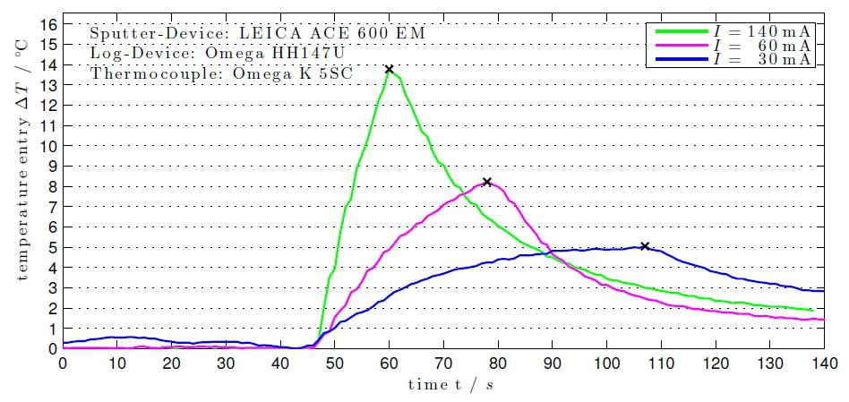
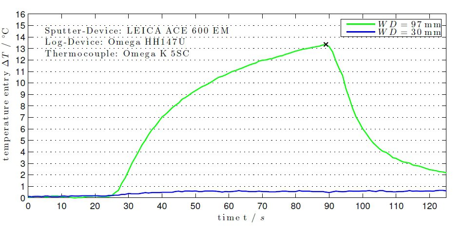
Fig. 4: Temperature increase as function of time by variation of the sputter current (upper) and the working distance (lower).
Besides the local temperature increase at the sample, the thickness values which are displayed during the sputter process were verified to check how precisely thin films are sputtered by Leica Microsystems’ sputter coater. Therefore, a multilayer system with different thickness values is sputtered which consists of two different materials. In this case, gold (Au) and tungsten (W) are used because the difference of the atomic number is adequate to get a good material contrast by the following TEM investigations.
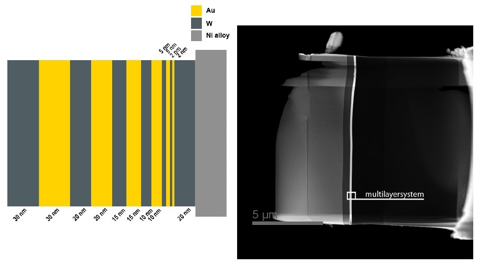
Fig. 5: Schematic of the electron transparent lamella based on a multilayer system of W and Au (left) and a TEM image of the lamella.
Another reason to choose these target materials was the fact that the characteristic x-ray peaks, which have the highest intensities, do not overlap and an EDX line scan can be performed through the multilayer system. Out of the EDX line scan the thickness values can be measured and compared by the result of the built-in quartz. The results can be seen in Table 1.
| Material | dLeica [nm] | dmeasured [nm] | dmeasured – dLeica [%] |
|---|---|---|---|
| W | 30 | 26.9 | 10.3 |
| Au | 30 | 28.5 | 5.0 |
| W | 20 | 20.7 | 3.5 |
| Au | 20 | 19.9 | 0.5 |
| W | 15 | 15.1 | 0.6 |
| Au | 15 | 14.5 | 3.3 |
| W | 10 | 10.5 | 5 |
| Au | 10 | 9.2 | 8 |
| W | 5 | 6.1 | 22 |
| Au | 5 | 5.0 | 0 |
Tab. 1: Comparison of the measured thickness and the expectation value. dLeica = setted thickness, whereat the sputter process will stop in nm; dmeasured = arithmetic averaged thickness value of all measurement methods in nm; dmeasured – dLeica = difference between expectation value and measured value in %.
Improvement of the sputtered films
To get a smooth and even surface, the sputter parameters which have the most influence on the film growth are systematically varied.
Thickness, working distance, current and argon pressure are changed in a certain range. The effect on the morphology by changing these parameters is more precisely described in [6]. The most important parameter which changes the morphology of the thin film is the argon pressure in the chamber of the coater. A decreasing of the argon pressure to values below 1e–2 mbar leads to a even film abruptly. This behaviour was observed for different target materials and it was shown that this effect is independent of the used target and also the critical argon pressure is nearly the same for every material.
To understand the physics behind the formation of the even film by sputtering at lower argon pressure, the film growth of a thin film which is sputtered with ditches and without ditches was compared and observed by TEM investigations (see Figure 6). Based on these findings the sputtered layer must be at least 2 nm thick to get an even film and the growth of thin films which are sputtered at higher argon pressure gets stopped at this stage where secondary nucleation should appear.

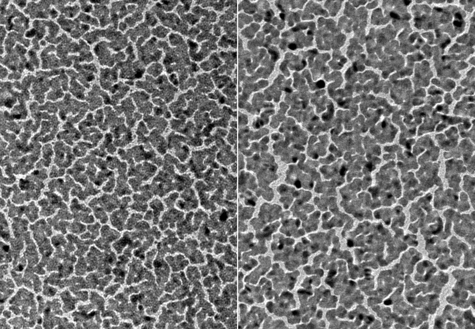
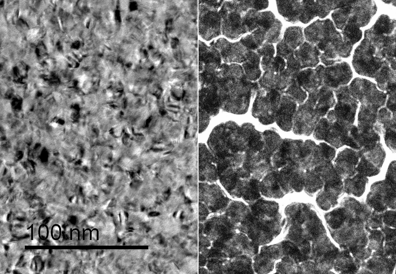
Fig. 6: TEM – Brightfield image (FEI Tecnai F20, zero loss filtered); left: 8e–3 mbar pressure; right: 5e–2 mbar. a) 0.5 nm, b) 1 nm, c) 10 nm.
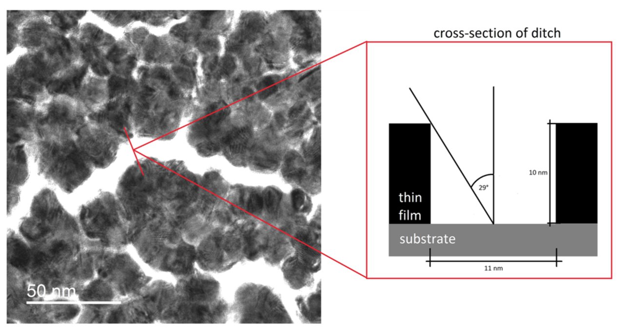
Fig. 7: Brightfield – TEM image (left): Film growth stages of Au/Pd at 10 nm and p=5e–2 mbar, FEI Tecnai F20, 200 kV. Schematic of ditch (right): Cross-sectional view at the ditch and calculated critical half-angle.
Low Argon pressure (p < 1e–2 mbar) leads to a smaller number of argon atoms in the chamber and therefore the amount of collisions between target atoms and argon atoms is reduced, the scattering angle is smaller and the kinetic energy of the target atoms is lower. Because of this smaller scattering angle the target atoms fall into the ditches which lead to secondary nucleation till the ditches are filled (see Figure 7, [3]). Additionally, the kinetic energy of the target atoms increases as well and this influences the mobility of the adatoms.
Characterisation of grown films
After the ability to sputter even metallic thin films, the quality of those films has to be quantised. Every film surface has characteristic dimensions of the formed islands. Therefore, atomic force microscopy was used to observe the topography of the films and measure the dimensions to express a quantity and evaluate the best material for HR-SEM applications.
To extract these dimensions from the AFM measurements several numerical methods were evaluated, like particle analysis tools by using the threshold technique, the power spectral density function, the radial autocorrelation function and an image processing tool based on the watershed algorithm. The sizes of such islands are in the nanometer range, hence a high lateral resolution has to be chosen for the quantisation. The resolution of the AFM image is set to the following conditions: 500 nm by 1024 px. Higher resolution would be possible but not applicable in this case of such small dimensions, because it would lead to drift effects which falsify the result of the lateral dimension (three examples of these images can be seen in Figure 8).
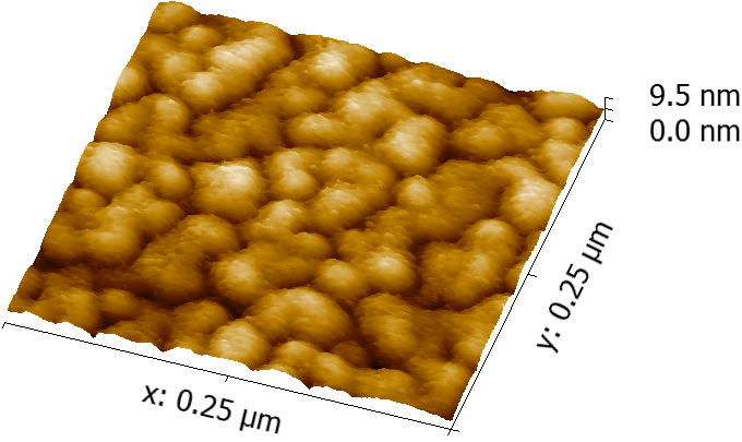
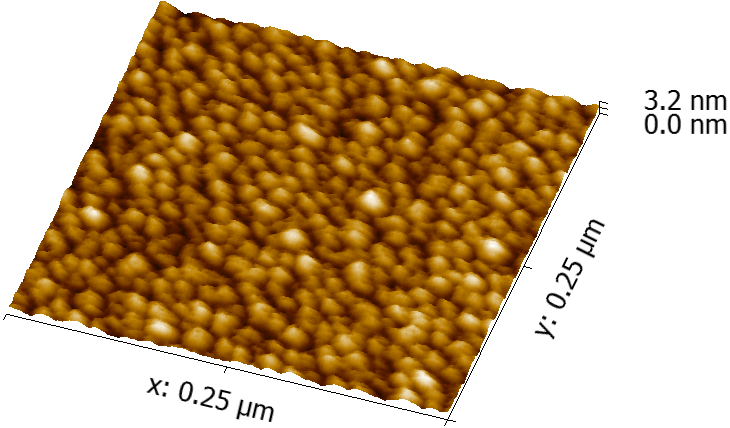
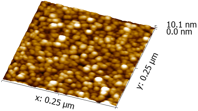
Fig. 8: AFM measurements (Bruker – Dimension FastScan Bio): a) Au layer 10 nm; b) Au/Pd 10 nm; c) Pt/Pd 10 nm
With this image processing tool and also with manual measurements of 100 different islands, a ranking of the mean island radius for different target materials was calculated (see Table 2). Besides the determination of the mean island radius, the roughness average value Ra and the ten-point height value RZ were used to estimate the height values of the islands. To get an even film a layer thickness of at least 2 nm is necessary for plane sample and the planetary drive stage and 5 nm for highly structured samples. The WD distance can be varied between 30 and 100 mm. At lower working distance the layer growth but also the heat impact in increased. The minimum sputter current for a stable plasma for different material is also shown in Table 2.
| Material | Island radius [nm] | Ra [nm] | RZ [nm] | pAr [mbar] | WD [mm] | Current [mA] |
|---|---|---|---|---|---|---|
| Au | 13.5 | 0.74 | 3.7 | < 1e–2 | 30–100 | > 15 mA |
| W | 8.3 | 0.14 | 0.7 | < 1e–2 | 30–100 | > 90 mA |
| Pt | 5.9 | 0.37 | 1.6 | < 1e–2 | 30–100 | > 15 mA |
| Au/Pd | 5.7 | 0.24 | 1.3 | < 1e–2 | 30–100 | > 15 mA |
| Pt/Pd | 5.3 | 0.18 | 0.9 | < 1e–2 | 30–100 | > 15 mA |
| Ir | 4.2 | 0.20 | 0.7 | < 1e–2 | 30–100 | > 80 mA |
Table 2: Summary of the optimized sputter parameters. Material = material of sputtered target; Island radius = mean island radius in nm; Ra = roughness average in nm; RZ = ten-point height in nm; PAr = Argon pressure in mbar; WD = working distance in mm; Current = sputter current in mA.
Application
Highly demanding samples concerning sputtering processes are lipids. They are biological and non-conductive samples which are highly temperature sensitive. The surface structure of lipids is most important for the different applications, what makes the Leica Microsystems DC magnetron sputter coater to the ideal device to sputter a thin conductive layer. In Figure 9 a completely artefact free high resolution SEM image of a highly structured pharmaceutical lipid sample is shown (10 nm Au/Pd sputtered).
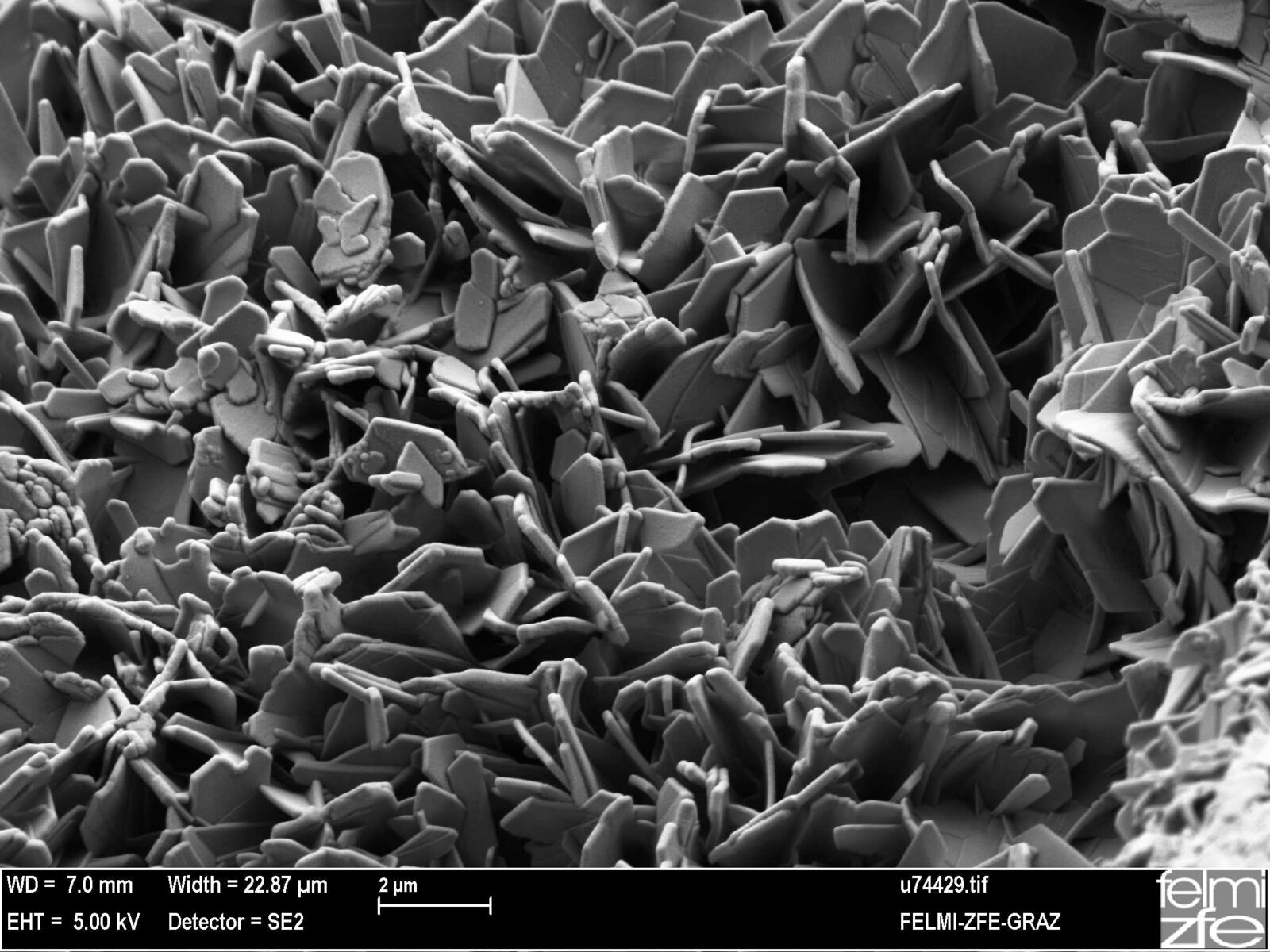
Fig. 9: Highly structured pharmaceutical lipid sample covered with 10 nm Au/Pd.
References
- Depla D, Mahieu S, and Greene JE: Sputter Deposition Processes.
- Venables JA: Introduction to surface and thin film processes. Cambridge, UK – New York: Cambridge University Press, 2000.
- Eisenmenger-Sittner C: Lecture notes of “Technologie Dünner Schichten”.
- Bertrand G: On topological watersheds. Journal of Mathematical Imaging and Vision 22 (2–3): 217–230 (2005).
- Melischnig A: DC magnetron sputtered thin films for HR-SEM.
Related Articles
-
-b-poly(isoprene). Right: Poly(styrene)-b-poly(methyl methacrylate).")
Ultramicrotome Sectioning of Polymers for TEM Analysis
We demonstrate the capabilities of the UC Enuity ultramicrotome from Leica Microsystems for…
Sep 30, 2025Read article -

Volume EM and AI Image Analysis
The article outlines a detailed workflow for studying biological tissues in three dimensions using…
Sep 16, 2025Read article -

Integrated Serial Sectioning and Cryo-EM Workflows for 3D Biological Imaging
This on-demand webinar explores how integrated tools can support electron microscopy workflows from…
Jul 22, 2025Read article
Related Pages
-

Electron Microscope Sample Preparation
Excellent sample preparation is the prerequisite for first-class electron microscopy. Be prepared –…
Visit related page
