

Why is cross-sectional analysis done?
Cross-section analysis is used to identify defects and study the integrity of PCB substrate materials and their layers [4], IC materials, electronic and battery components [3,5], solder joints [1,4], voids, and cracks [1].
By making a precise cross sectional cut perpendicularly across the area of interest of the PCB or IC, the internal structure of the bulk volume, the thickness and homogeneity of different layers, and potential defects and failure mechanisms can be examined and analyzed using a variety of methods. Examples include optical and electron microscopy, energy dispersive X-ray spectroscopy (EDS), and laser-induced breakdown spectroscopy (LIBS) [3-5].
These methods enable precise visualization and targeted chemical analysis of specific internal areas within the cross section of a sample. These techniques can be important for QC during production, investigating failure mechanisms when doing FA, or the R&D of new components.
Challenges of preparing cross sections
PCBs, ICs, and battery components are “mixed” or “multi-phase composite” materials (composed of metals, ceramics, and polymers) which pose certain challenges for cross-section preparation. The problem is deformation or damage, as each material has different mechanical properties leading to a variation in grinding, polishing, and milling behavior. As a result, cross section surfaces can have defects, like scratches or lines, be irregular and rough, or show smearing of soft materials which may cover and obscure structures of interest, such as pores and voids. These troubles can lead to poor quality.
Preparation of material cross sections
The preparation of cross sections from PCBs, ICs, and battery components involves several techniques and the following steps [2-6]:
- Selecting a representative area of the board or component;
- Removing any encapsulation and protective layers that may be present;
- Mounting the sample:
- When preparing by hand, mounting it in a suitable material, such as an epoxy or resin, to provide stability for cutting and polishing;
- When using a mechanical grinding/polishing/milling or ion-beam milling system from Leica Microsystems, glue it to the sample holder;
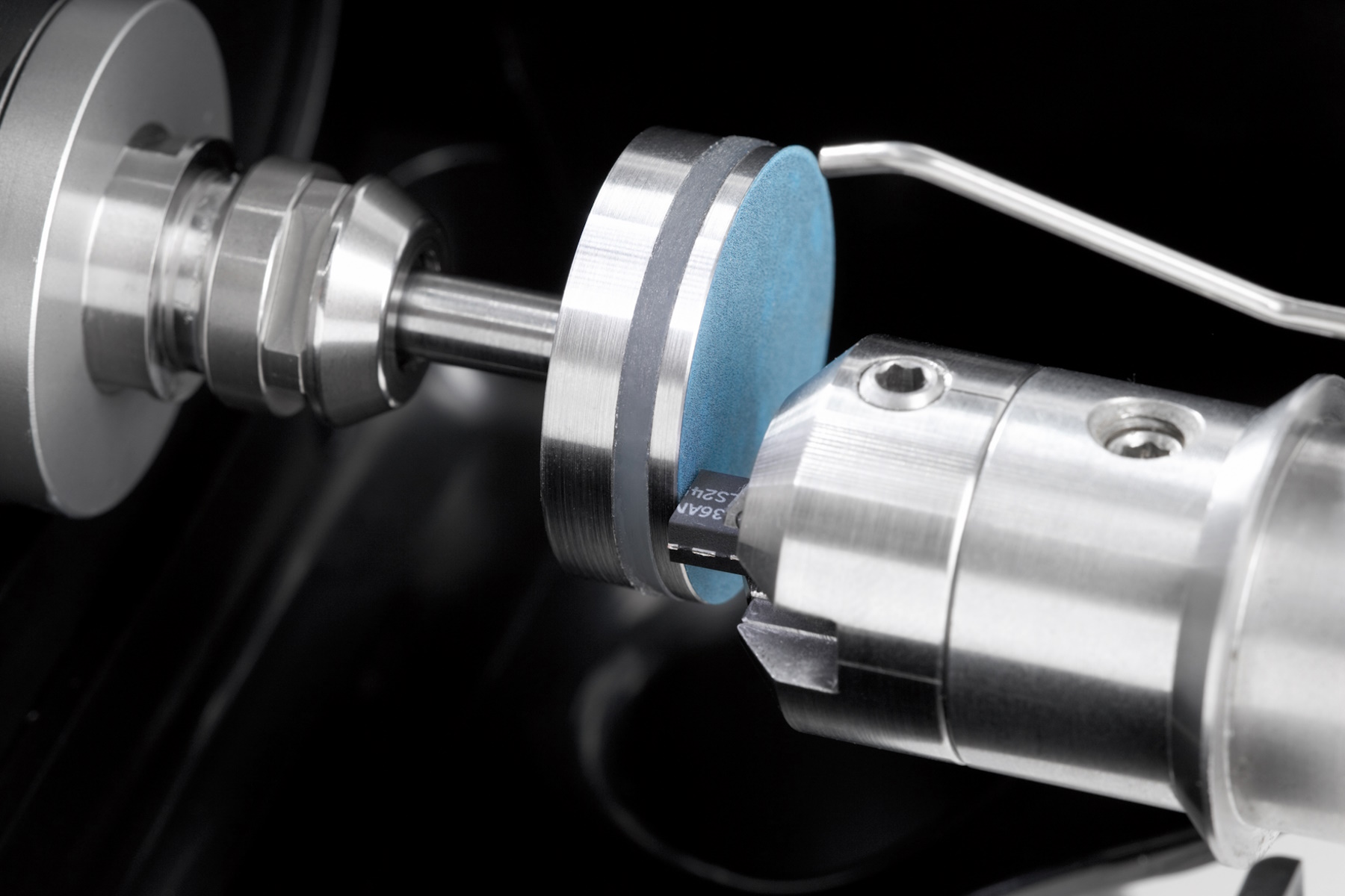
- Cutting or slicing via mechanical sawing or ion-beam milling for brittle materials to obtain a cross section providing access to the desired layers and internal structure;
- Grinding, polishing, or milling of the cross section to obtain a flat, smooth, and clean surface (crucial for high-resolution imaging with microscopy):
- When preparing by hand, such as with a turntable, use progressively finer grades of abrasives like silicon-carbide paper and diamond paste or suspensions on a soft cloth;
- When using a mechanical grinding/polishing/milling or ion-beam milling system, follow the recommendations provided by the manufacturer;
- Selective etching to highlight specific grains, elements, and layers; and
- Analyzing the cross section visually and chemically using microscopy and spectroscopy.
Advantages of mechanical grinding/polishing/milling or ion-beam milling systems
When comparing cross-section preparation using a mechanical grinding/polishing/milling or ion-beam milling system versus grinding and polishing by hand, there are certain advantages [5,6]:
- Total time needed with mechanical or ion-beam milling systems is typically 1 to 2 hours, while hand preparation can require several hours or even 1 to 2 days;
- Quality of cross sections is often higher with mechanical systems, as there are less scratches and fewer defects unlike hand preparation; and
- Quality of cross sections is much higher with ion-beam milling, as there are no scratches and smearing and much fewer artifacts, unlike preparation by hand or with mechanical systems.
 chip mounted on the sample holder, B) sawing of the chip to expose the cross section, C) grinding and polishing of the chip cross section, and D) final image of the prepared chip cross section.")
Cross-section analysis techniques
Techniques like optical microscopy, scanning electron microscopy (SEM), LIBS, or EDS can be used for detailed visual and chemical analysis of a cross section.
An optical microscope with LIBS can be used to image a cross section’s fine details and microstructure and analyze their composition (refer to figure 3). LIBS enables qualitative chemical analysis of small, specific areas of the cross section in seconds and does not require extra sample preparation [7].
If no compositional information of the microstructure is required, and multiple samples of different heights must be analyzed, then a practical advantage can be attained by using an inverted optical microscope.
A SEM is capable of higher magnification than an optical microscope. It also can provide both image and elemental data (EDS) for the details and microstructure of a cross-section.

Leica solutions for cross-section preparation and analysis
Cross sections of PCBs, PCBAs, ICs, and battery components can be prepared rapidly and reliably using the:
- EM TXP solution for milling, sawing, grinding, and polishing enabling quick and easy preparation of samples to be analyzed with microscopy and spectroscopy; and
- EM TIC 3X solution for ion-beam milling TIC 3X required when more demanding surface analysis is needed, such as with SEM, EDS, and EBSD (electron backscatter diffraction) [8].
If an inert atmosphere, vacuum, or controlled temperature is required for sample preparation and transfer, as can be the case during battery R&D, this aim can be achieved with the TXP system inside a glovebox as well as the TIC 3X used in conjunction with the VCT500 transfer system.
Efficient and accurate visual and chemical analysis of cross sections can be done with the DM6 M LIBS 2-methods-in-1 solution combining optical microscopy and LIBS.
Summary and conclusions
Cross-sectional analysis is useful for quality control, failure analysis, and R&D of electronic components like printed circuit boards (PCBs) and assemblies (PCBAs), integrated circuits (ICs), and batteries. It enables accurate evaluation of the structural integrity of the layers and materials and identification of defects and potential failure mechanisms.
Cross-section analysis is a multi-step process which requires precise sample cutting and preparation in order to obtain a smooth, flat, and clean surface. Observation and analysis is performed using methods like optical microscopy, SEM, EDS, and LIBS which allow both high-resolution imaging and determination of elemental composition.
 at the edge of a battery electrode acquired with a DVM6 digital microscope.")
 chip cross section acquired at higher magnification showing a region of interest.")