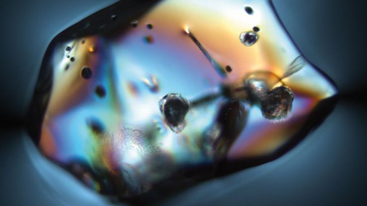
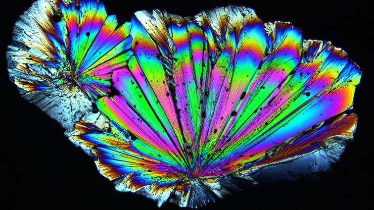
Ensuring Glass Quality with the Polarization Microscopy Advantage
Glass is one of the oldest materials known. Today, it is used for many applications, e.g., optical instruments, windows, doors, solar panels, containers for food, beverages, and medicine, so strict…
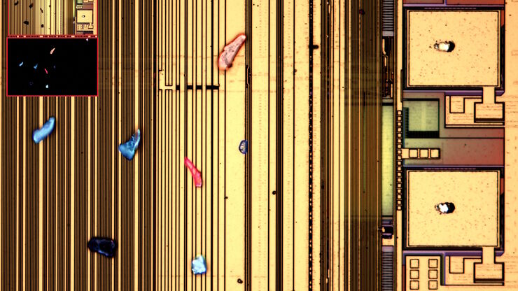
Visualizing Photoresist Residue and Organic Contamination on Wafers
As the scale of integrated circuits (ICs) on semiconductors passes below 10 nm, efficient detection of organic contamination, like photoresist residue, and defects during wafer inspection is becoming…
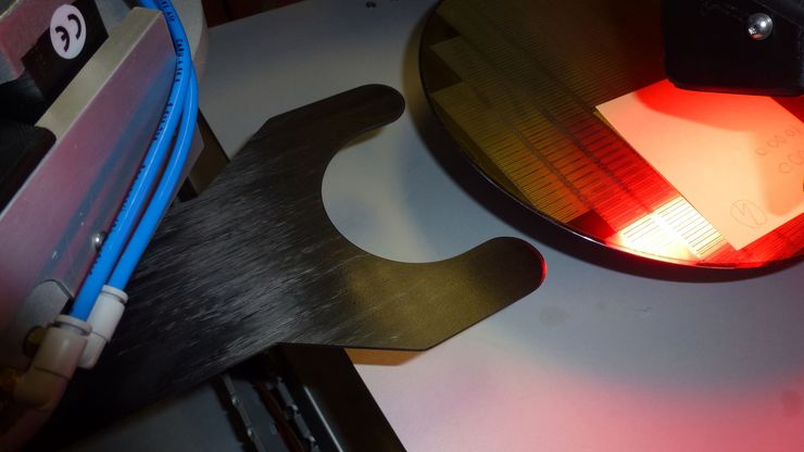
Safe Wafer Loading for Microscope Inspection without Hand Contact
How automated silicon wafer loading for microscope inspection helps improve microelectronics process control and production efficiency is explained in this article. Manual handling of wafers has a…
Burr Detection During Battery Manufacturing
See how optical microscopy can be used for burr detection on battery electrodes and determination of damage potential to achieve rapid and reliable quality control during battery manufacturing.
Quality Assurance Improvement Across Industries
Precision is paramount. Imagine a pacemaker that fails mid-operation or a semiconductor flaw that causes a critical system crash. In industries, such as medical devices, electronics, and…
Polarizing Microscope Image Gallery
How polarization microscope images can be used for analysis is shown in this gallery. Polarized light microscopy (also known as polarizing microscopy) is an important method for different fields and…
Automotive Part Verification and Development according to Specifications
Automotive part verification during the development and production of parts and components by suppliers or manufacturers is important for ensuring that specifications are met. Specifications are…
Battery Particle Detection During the Production Process
How battery particle detection and analysis is enhanced with optical microscopy and laser spectroscopy for rapid, reliable, and cost-effective QC during battery production is explained in this…
Key Factors for Efficient Cleanliness Analysis
An overview of the key factors necessary for technical cleanliness and efficient cleanliness analysis concerning automotive and electronics manufacturing and production is provided in this article.

