Contact Us

Structural and Chemical Analysis of IC-Chip Cross Sections

Workflow optimization for advanced materials analysis concerning applications in the electronics industry

Image of an integrated-circuit (IC) 
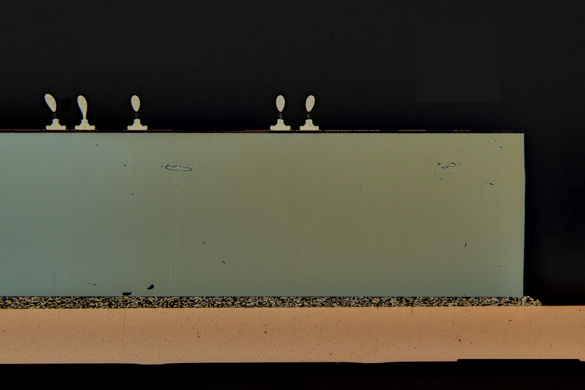
chip cross section acquired at higher magnification showing a region of interest. IC_chip_cross_section.jpg

Find out from this article how structural and elemental evaluation can be performed efficiently on electronic components like integrated-circuit (IC) chip cross sections. It is done using a surface targeting system for milling, sawing, grinding, and polishing and a 2-methods-in-1 solution for simultaneous visual and chemical analysis. Rapid, detailed material analysis can be achieved for a variety of workflows and applications in the electronics industry, including competitive analysis, quality control (QC), failure analysis (FA), and research and development (R&D).

For the electronics industry, sometimes destructive sample preparation is necessary when performing QC (quality control), failure analysis, R&D (research and development), and competitive analysis of components like integrated-circuit (IC) chips. In many cases, a cross section of the electronic component is made and then the internal structure and chemical composition is analyzed.

For the investigation reported here, the cross section of an IC chip was prepared with the EM TXP target surfacing system. With the EM TXP, samples can be mechanically milled, sawed, ground, and polished prior to microscopy and spectroscopy examination. The chip cross section was then analyzed for both internal structure and composition using the DM6 M LIBS 2-methods-in-1 material analysis solution. The DM6 M LIBS combines both high-resolution optical microscopy and laser-induced breakdown spectroscopy (LIBS), enabling structural and chemical analysis to be done at the same time.

The results presented show how an efficient overall workflow for advanced materials analysis of IC-chip cross sections can be achieved with the EM TXP and DM6 M LIBS solutions. The same workflow and solutions can be applied to other electronic components as well.

Key Learnings

This article provides users with:

  • A step-by-step guide for the workflow concerning IC-chip cross sectioning as well as visual and chemical analysis
  • Tips on using a target surfacing system for quick, reliable sample preparation of chip cross sections
  • An example of efficient and reliable visual and chemical analysis of chip cross sections
  • References to useful publications concerning advanced materials analysis of electronic components

Download Application Note

By clicking on the SUBMIT button, I confirm that I have reviewed and agree with Leica Microsystems GmbH Terms of Use and their Privacy Policy. I also understand my privacy choices as they pertain to my personal data, as detailed in the aforementioned Privacy Policy under ‘’Your Privacy Choices’’.

Related Articles

Background image
Scroll to top