. The grains are highlighted with arbitrary colors.")
What is EBSD analysis?
Electron backscatter diffraction (EBSD) is a SEM (scanning electron microscopy) technique which can be used to investigate the microstructure of crystalline materials down to the nanoscale [1-5]. It is referred to as a "surface" technique, because diffraction of the backscattered electrons occurs only within tens of nanometers just below the sample surface. Reliable EBSD analysis depends greatly on high-quality sample preparation so that good Kikuchi patterns are obtained. Therefore, to obtain these patterns, the sample surface should be crystalline and have no damage or contamination resulting from the preparation.
Challenges of EBSD sample preparation
To prepare regions or cross-sections of a material for SEM-based analysis, often focused ion-beam (FIB) milling is used. However, this method is rather slow, requires a lot of expertise, and has significant limitations when preparing large areas of multiphase composite materials for EBSD. Because FIB can cause significant localized heating and damage, it changes significantly the local surface structure of the sample compared to the bulk. This effect is especially problematic for multiphase composite materials, as each material has different properties and milling behavior. FIB preparation can result in varying thicknesses for each type of material in the composite and cause the resulting sample surface to have lines or be irregular and rough (curtaining effect) [6].
Methods
Materials
The samples analyzed were:
- Highly deformed gold (Au) wires from an integrated circuit of a CPU (central processing unit) which were embedded in a silicon (Si) matrix with tungsten (W) [7] (refer to figure 1a) and
- A composite material with an aluminum (Al) matrix containing diamond grains and graphite flakes (refer to figure 1b) [7].
Cross sections of the samples were prepared with the methods described below.
 Photo of the PCBA from which the gold-wire sample (IC in the CPU) was acquired. b) Overview SEM image, showing the sample surface of the Al/diamond/graphite composite material, taken with secondary emission of electrons.")
Cross sectioning by slope cutting with broad ion-beam (BIB) milling
Sample cross sections were prepared by first using sawing, then mechanical grinding and polishing, down to 1 µm, with the EM TXP system (refer to figure 2a), which allowed the area of interest to be reached in a very short time [7]. Then, BIB milling was performed using the EM TIC 3X system (refer to figure 2b), to attain a cross section with a high-quality surface ready for EBSD analysis [7,8].
 To reach the area of interest, basic cross sectioning was done for 20 minutes with the EM TXP. b) Then, to have a high-quality cross-section surface, broad ion-beam milling was performed with the EM TIC 3X.")
Imaging and analysis
Phase- and orientation-contrast SEM imaging and the corresponding EBSD microstructural analysis of the sample cross sections were done with an ARGUS™ FSE/BSE (forward-scattered/backscattered electron) system and eFlash detector [7].
Results
Electronic component: CPU
The EBSD analysis was done over a large area of the gold wires where they were plastically deformed during bonding within the IC of the CPU [7] (refer to figure 3a). FSE (forward-scattered electron) images, useful for crystallographic orientation contrast, reveal that there is a bit of a curtaining effect, however, none of the map data, specifically the EBSD-misorientation average and kernel maps, show any appreciable curtaining, i.e., there is no structure which follows the curtaining effect (refer to figure 3 below). Therefore, both EBSD and EDS (energy dispersive x-ray spectroscopy) analysis indicate that BIB milling enables a high-quality cross-section surface to be prepared, as it did not cause any noticeable sub-surface damage.

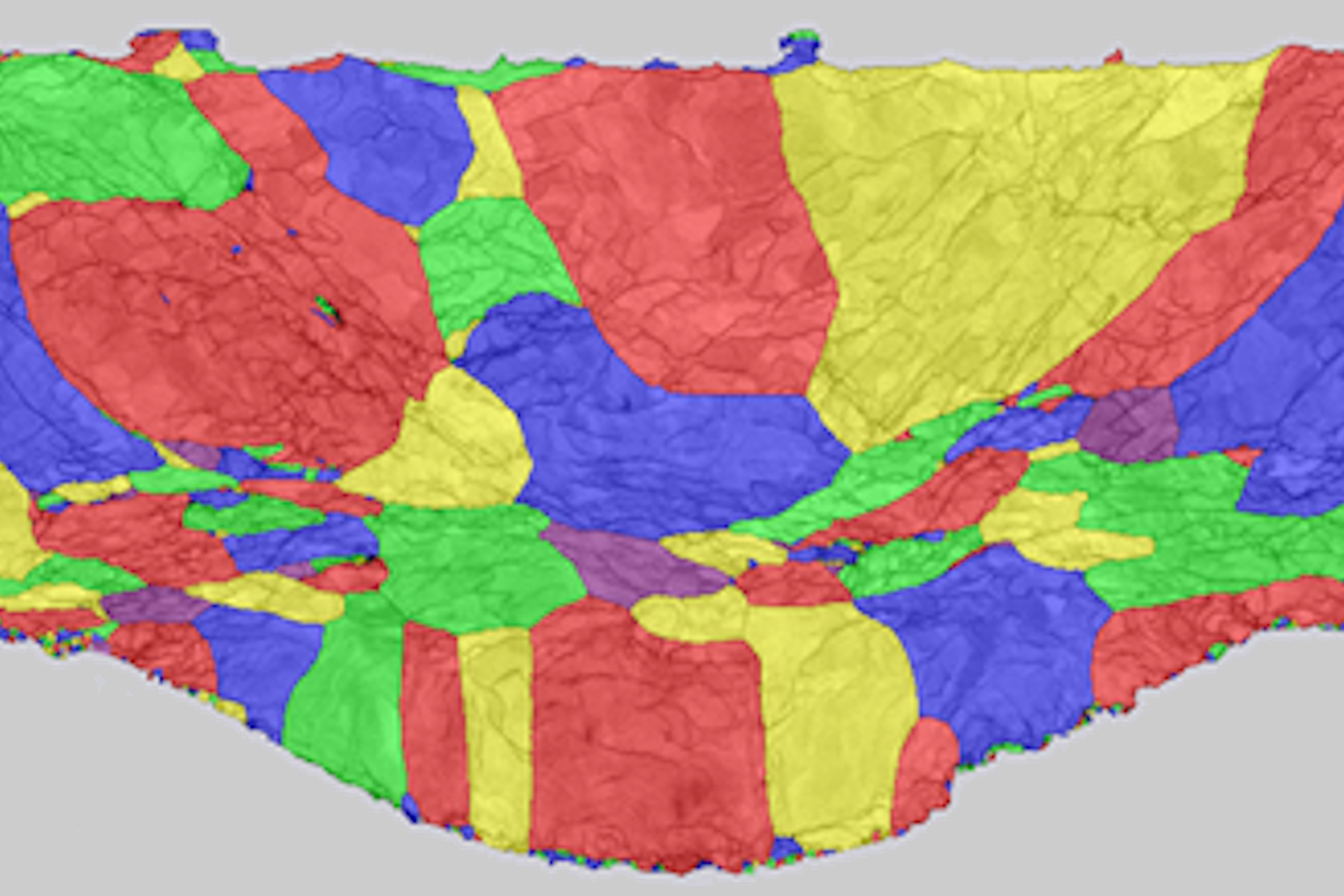
Composite material: aluminum/diamond/graphite
The Al/diamond/graphite composite cross section was examined using BSE imaging, EDS (energy dispersive x-ray spectroscopy), and EBSD with phase and inverse pole figure (IPF) maps along the X (tilt) axis [7]. The results reveal a high-quality surface preparation of the Al matrix containing graphite flakes and diamond grains with no appreciable curtaining effect over a region 3 mm in size (refer to figure 4 below). The EBSD phase and orientation maps confirm this result, as the 3 different phases were successfully indexed despite producing similar diffraction patterns. The combination of well-prepared sample surfaces and simultaneous acquisition of EBSD and EDS data made this analysis successful.

Conclusions
Although the focused-ion-beam (FIB) technique is often used for site-specific preparation of a wide range of materials, successful EBSD analysis of FIB-prepared samples can be quite challenging due to the introduction of sub-surface deformation and curtaining. This fact is especially true for multiphase composite materials having regions with varying hardness. Here, it was demonstrated that broad ion-beam (BIB) milling allows a high-quality, simultaneous preparation of both hard and soft materials in a composite. The combined use of the EM TXP and the EM TIC 3X enables users to prepare high-quality, large-area samples from very challenging composite (multiphase) crystalline materials in a short time . EBSD analysis of samples prepared with BIB-milling often yields useful results [7-10].
Acknowledgements
We would like to thank Andi Kaeppel and Dr. Roald Tagle of Bruker Nano GmbH in Berlin for contributing the photo of the gold-wire-bonded CPU processor shown in figure 3a and Dr. Gang Ji at the Université de Lille in France for providing samples of the Al/diamond/graphite composite material.


-b-poly(isoprene). Right: Poly(styrene)-b-poly(methyl methacrylate).")
