Why is a wafer loader useful for microscope inspection?
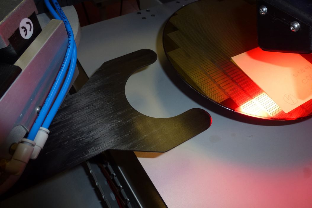
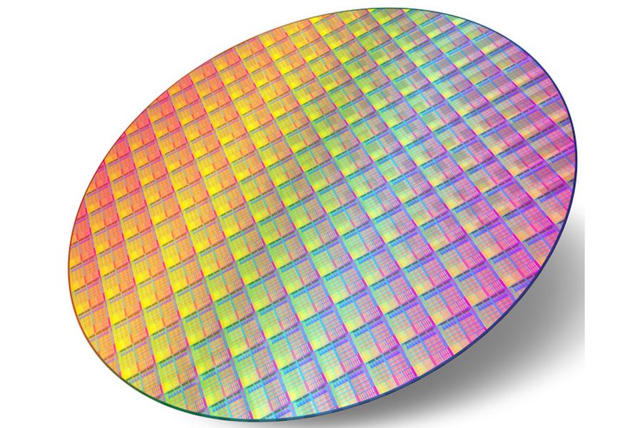
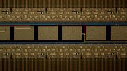
In production environments, silicon wafers (see figure 1) should not be manually handled with instruments such as tweezers. Manual handling is permissible only for certain laboratory applications. It is imperative that wafers remain undamaged during inspection, as rectifying damaged wafers in the production process is both complex and costly. Given that wafers are fragile and expensive, automated handling is typically required. For production, particularly during initial stages where limited areas of the wafer surface are inspected with a microscope, the priority is not just processing speed, but also reliability and wafer protection. These requirements cannot be reliably met with manual handling. Consequently, automated wafer loading procedures [1,2] must be implemented for microscope inspection.
What are the advantages when using a wafer loader?
Related to the challenges mentioned above, the main advantage offered by wafer loaders is improved process control. A loader can be integrated into a factory production line and enable better control over the production flow. Also, it can be used with assisted inspection stations to help operators perform defect classification and report generation. Another issue addressed with loaders is related to critical wafer handling. Some wafers, such as, TAIKO® wafers [3], where the thickness at the edges is 3 or 4 mm thick and at the center is 50 µm or less, simply cannot be manually handled. Other issues can be related to thin wafers which are warped meaning the wafer surface is like a “potato chip” with up to 6 mm of warpage. For such cases, not only is the use of a wafer loader critical to take wafers out of and put them back into the carrier, but also the movable ring supports on the DM8000 microscope vacuum chuck which keeps the wafers flat for inspection [4].
Solution for effective wafer loading
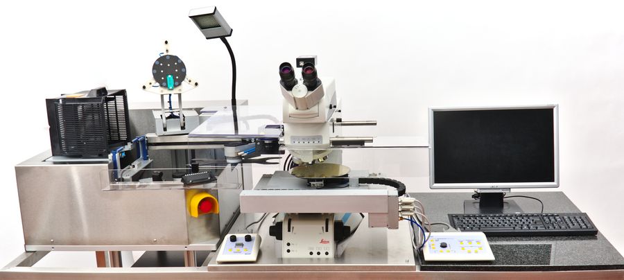
The MIL8000 wafer autoloader and macro inspection station from Semisyn - Astel [5] is an effective system for automatically loading wafers onto a microscope to perform front and backside macro inspection. It has been designed to work with the DM8000 microscope [6] from Leica Microsystems (see figure 2). The MIL8000 is compact, so wafer loading can be done without complex interfaces nor special microscope stages. Efficient macro inspection is done with LED illumination. Wafer backside inspection is done with a contactless Bernoulli unit which allows the whole surface to be inspected in a single operation. An example of wafer inspection with the MIL8000 is shown in reference 7.
Microscope solution for efficient wafer inspection
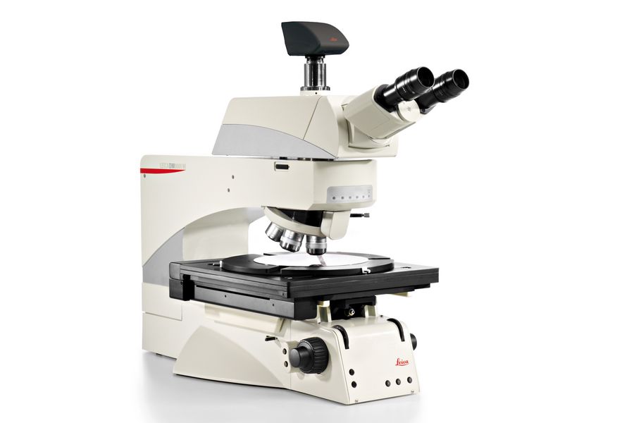
The DM8000 microscope (see figure 3) helps make wafer inspection quick and reliable thanks to automation, user-friendly operation, and an ergonomic design [6]. Various structures and defects, such as scratches and contamination on wafers can be efficiently detected and analysed using the array of illumination and contrast methods available. Examples include brightfield, darkfield, polarization, differential interference contrast (DIC), oblique illumination, ultraviolet (UV), infrared (IR), and fluorescence [8-10]. There is a variety of accessories available for the microscope, like a special vacuum wafer chuck that keeps them flat during inspection.

