An efficient way to protect any sample is to deposit an interstitial carbon protection layer with a uniform density and thickness. Conventional carbon rod evaporation will impart a considerable amount of heat on the sample causing damage.
Adaptive carbon thread evaporation, on the other hand, will form a strong and conductive layer while maintaining the pristine characteristics of the sample. This new evaporation mode which was already well received by the scientific community is characterized by its superior flexibility and high reproducibility. It enables its users to deposit a uniform and conductive carbon layer with minimal impact on the sample. Moreover, its low sputter rate and absolute absence of grain structures allows an optimal protection and a decrease of curtaining effects respectively.
This application note discusses protective coatings and shows the most optimal route to protect your samples and the rule out any doubts concerning the fine structure of the surface up to the atomic level.
Permanent marker deposition was suggested as a mean to protect samples against focused ion beam damage by simply drawing a line on the sample using a black-colored permanent marker. Although very fast and cheap, such layers are not reproducible and thick layers often obscure a clear visualization of the sample surface prior to FIB milling. Hence, they hamper a fast localization of the correct region of interest. Moreover, it is ofen unclear how those layers will react once exposed to high probe currents often using during atomic resolution STEM imaging or prolonged EELS data acquisitions. The resin used in the permanent marker ink can outgas and be a potential source of contamination, especially when performing atomic resolution imaging or spectroscopy. The applied layers are also rather polymeric and are considerably less conductive.
As an alternative, amorphous carbon coating can be used as a protective layer. Although carbon can be deposited by a range of different deposition modes, this application poses some stringent demands on the quality of the layer. In order to be suited for this application, the carbon layer should be: (1) of a uniform density, (2) conductive, (3) have a low impact on the sample during deposition and (4) be free of any particulate matter.
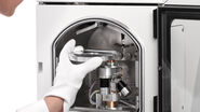
Adaptive carbon thread is an efficient way to deposit an amorphous carbon layer with minimal impact on the sample. Here, a carbon thread is placed along 5 electrical terminals allowing to evaporate 4 carbon thread segments completely. The adaptive process ensures a constant power output by measuring the resistance after each pulse and adaptingthe next power output accordingly. This process not only ensures a complete use of each thread segment without release of debris but also highly contributes to a superior carbon layer free of granular structures and density variations.
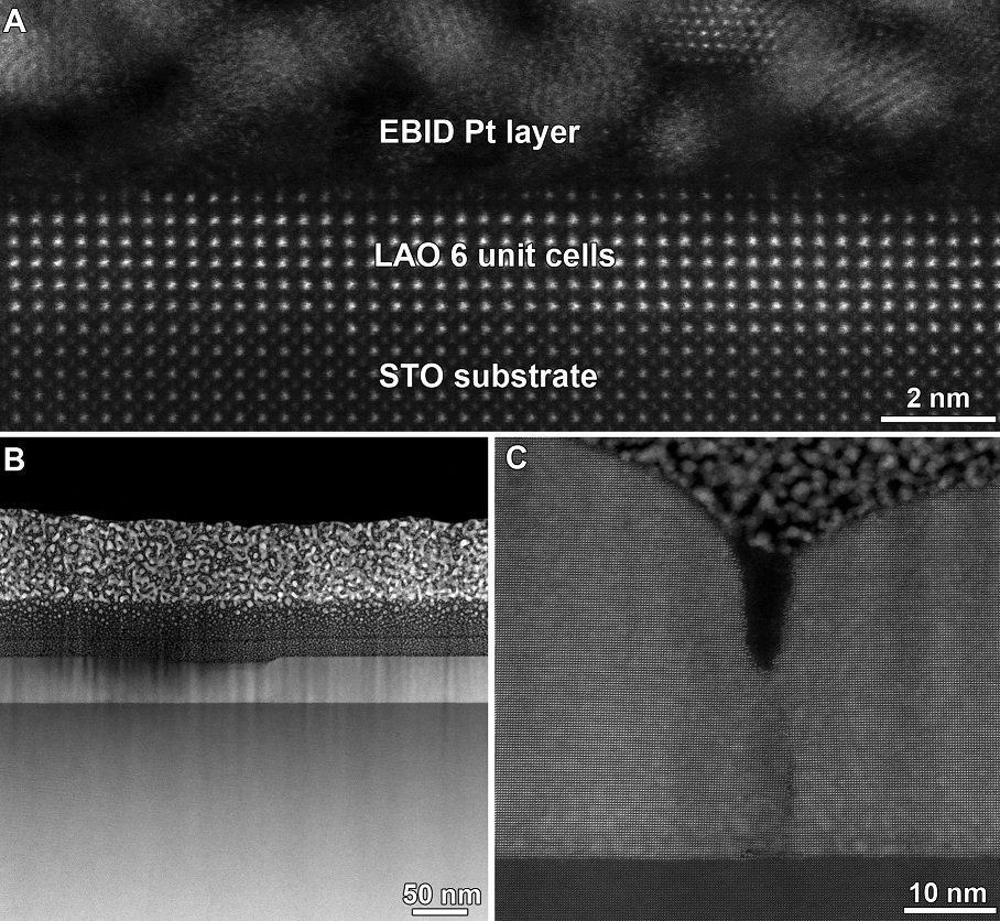
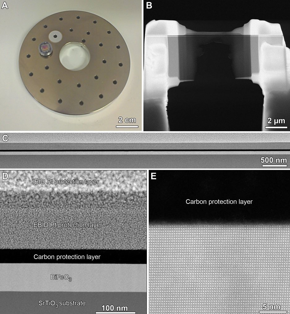
Because the process results in a low energy evaporant, atom intermixing does not occur at the surface of the sample. Figure 2A shows a SEM stub after a 35 nm carbon coating. Consecutively, EBID and IBID Pt layers were deposited locally after selecting the region of interest. Figure 2B shows the final TEM lamella mounted on an omniprobe grid. Figure 2C shows a uniform thickness of the carbon layer along the cross section. Here, the substrate and thin film are protected by the carbon layer onto which EBID and IBID layers were deposited. As a consequence, the surface atoms and layers are protected from FIB milling artefacts. The amorphous carbon protection layer can also be used to fine tune probe aberrations or serve as a reference layer for analytival TEM.
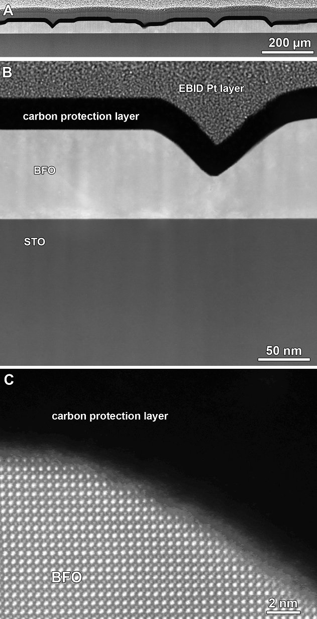
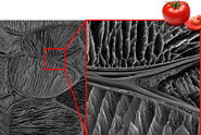
To illustrate the superior performance of the adaptive carbon thread coating in terms of diffuse and uniform coating, an irregular sample was protected with carbon (figure 3A). A uniform thickness can still be obtained a full protection is guaranteed along the surface of the sample up to atomic scale. The diffuse contrast on top of the first atomic layer in image 3C is due to atmospheric contamination. A larger amount of contaminants, however, can outgas during FIB imaging and can locally cause the carbon to bubble up. In such cases a cleaning step should be performed before FIB processing. This can be accomplished by glow discharge or plasma cleaning.
To conclude, adaptive carbon thread evaporation produces amorphous protection layers that are extremely suited against FIB milling damage and artefacts. Its lower sputter rate also protects the sample during FIB processing and ensures a complete protection of the surface and subsurface layers up to atomic scale.
Images acquired by Dr. Ricardo Evoagil and Prof. Dr. Jo Verbeeck, EMAT, University of Antwerp. EMAT is part of the ESTEEM2 consortium (www.esteem2.eu)
Related Articles
-
Sample Preparation for EM: A Practical Guide to Coating and Freeze-Fracturing
From coatings done in a low-vacuum sputter coating machine at room-temperature to those done in…
Feb 02, 2021Read article -
Studying the Microstructure of Natural Polymers in Fine Detail
The potential of cryogenic broad ion beam milling used in combination with scanning electron…
Oct 16, 2019Read article -

Expert Knowledge on High Pressure Freezing and Freeze Fracturing in the Cryo SEM Workflow
Get an insight in the working methods of the laboratory and learn about the advantages of Cryo SEM…
May 23, 2019Read article
Related Pages
-

Electron Microscope Sample Preparation
Excellent sample preparation is the prerequisite for first-class electron microscopy. Be prepared –…
Visit related page
