
As the scale of integrated circuits (ICs) on semiconductors passes below 10 nm, efficient detection of organic contamination, like photoresist residue, and defects during wafer inspection is becoming more crucial. Optical microscopy is still the common inspection method, but for organic contamination brightfield and other types of illumination can have limitations. How fluorescence microscopy is used to efficiently detect photoresist residues and other organic contamination on wafers during QC, failure analysis, and R&D for the semiconductor industry is discussed in this article.
Challenges when inspecting wafers for organic contamination and photoresist variation
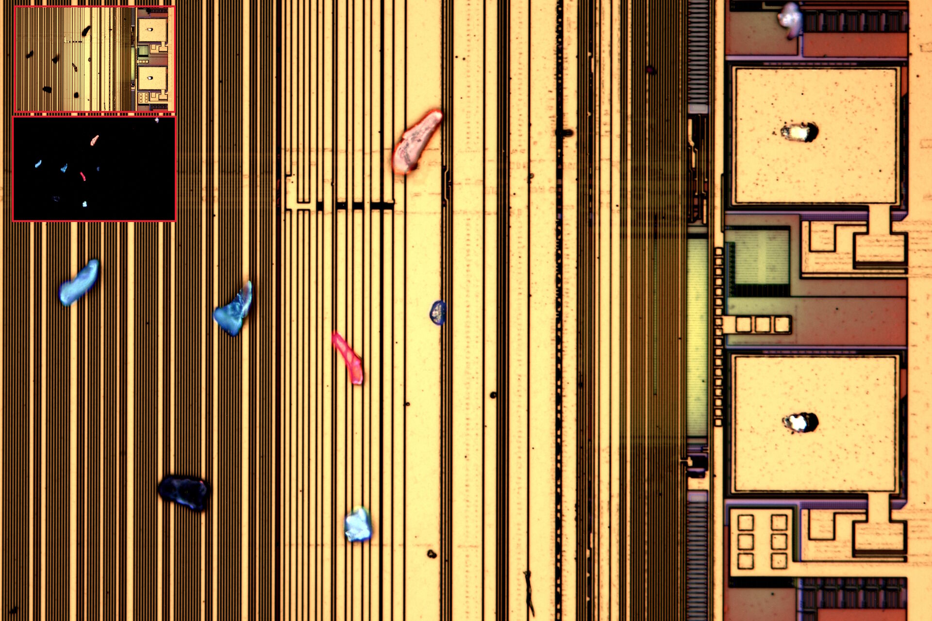
Efficient and reliable detection of photoresist residue and residual organic contamination with optical microscopy during wafer inspection can be challenging. Wafer inspection with an optical microscope often requires multiple contrast methods. These residues are not always easy to see with the more common microscope illuminations, e.g., brightfield or darkfield [5], depending on the volume of organic contamination (refer to figure 1). As
semiconductor patterning approaches nanoscale dimensions, even very small amounts of photoresist residue or other residual contamination can cause serious problems for further processing. This fact makes accurate wafer inspection with common microscope illuminations time-consuming and inefficient.
 brightfield, B) darkfield, and C) fluorescence illumination.")
Fluorescence microscopy and how it benefits the electronics and semiconductor industry
Fluorescence microscopy is a powerful tool for observing organic materials on wafers and semiconductors. It is based on the principle of photoluminescence where atoms and molecules are excited by a light of higher energy (shorter wavelength), e.g., ultraviolet (UV), and then relax by emitting light of lower energy (longer wavelength), such as light in the visible range [6]. The differences between fluorescence and brightfield microscopy are shown in figure 2. Examples where fluorescence microscopy is used for detection of photoresist residue and organic contamination as well as inspection of RGB pixels in OLED displays are mentioned in the following sub-sections.
 and brightfield (B) microscopy.")
Detecting photoresist residue and organic contamination during QC and R&D
Photoresist and many organic materials fluoresce after being excited with UV light. On the wafer surface, these materials can be more easily localized and quantified with fluorescence microscopy compared to typical microscope illumination like brightfield (refer to figure 3). So fluorescence microscopy can be exploited for wafer inspection and lead to efficient visualization of these organic residues, meaning reduced inspection times, higher throughput, and improved semiconductor component quality.
 brightfield illumination, B & E) fluorescence, and C & F) overlay of brightfield and fluorescence.")
Inspecting pixels of OLED displays
Another example where fluorescence microscopy can be useful is the production or inspection of OLED (organic light-emitting diode) displays. OLED displays are made of an array of RGB pixels consisting of one or more layers of light-emitting organic molecules within a stack (refer to figure 4) [7]. Layer uniformity and thickness are very important to maintain high pixel efficiency and quality and must be accurately monitored during fabrication. Also, there should be no gaps in the organic layer of RGB pixel molecules on the silver (Ag) coating. These organic molecules are also fluorescent. Thus, the quality of the RGB array output for OLED displays could be monitored in an efficient and reliable way using fluorescence microscopy (also can be done with non-fluorescence microscopy and electroluminescence) [refer to figure 5].
Leica fluorescence microscope solutions for wafer inspection
The DM8000 M (refer to figure 6), DM12000 M, and DM6 M microscopes are designed for inspecting 8-inch, 12-inch, and 6-inch wafers, large semiconductor components, and flat electronic components like OLED displays.
They offer users the following:
- Option for fluorescence microscopy when equipped with selected fluorescence cubes
- More efficient imaging with optional motorized versus manual operation
- Efficient wafer or component inspection with macroscopic inspection mode
- A variety of illumination and contrast methods including brightfield, darkfield, DIC, polarization, IR, oblique, and UV.
Thanks to the availability of multiple contrast and illumination techniques, including fluorescence, and a large magnification range, users can configure the DM8000, DM12000, or DM6 M as an inspection tool for their specific needs.

Conclusion
The growing demand for faster, smaller, and more complex ICs and semiconductor components requires fast and reliable methods of detecting organic contamination (photoresist residue, foreign organic particles and liquids) on wafers. Optical microscopy with multiple contrast methods, such as brightfield or darkfield, are typically used for wafer inspection, but are limited in terms of visualizing residual organic contamination, making inspection
time-consuming and inefficient. Here it was described how fluorescence microscopy can be used for an efficient wafer inspection concerning organic contamination during QC, failure analysis, and R&D for the semiconductor industry. In the future, the fact that organic contamination on wafer surfaces show different fluorescence signals, i.e., they fluorescence at different wavelengths and colors after being excited by UV light, means this phenomenon could be exploited to differentiate types of contamination. With a suitable fluorescence microscope, then “root cause analysis” can be done to determine the source of various organic contaminants.
. With DIC users are able to visualize small height differences on the wafer surface more easily.")


