. With DIC users are able to visualize small height differences on the wafer surface more easily.")
Introduction
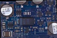
Wafer inspection during production of semiconductor components is essential for identifying and reducing defects which can affect component performance. To enhance inspection precision and efficiency, optical microscope solutions should combine different contrast methods that provide accurate and reliable information about any defects that may be present on the patterned wafer. One contrast method that plays an important role in wafer inspection is differential interference contrast (DIC).
What is DIC and why use it?
Differential interference contrast (DIC), also known as Nomarski contrast, helps to visualize height differences on a sample surface [1,2]. DIC uses a Wollaston prism, a polarizer, and an analyzer (refer to figure 1A). The polarization planes of the polarizer and analyzer are perpendicular (crossed at 90°) to each other. Polarized light passing through the prism is sheared into two waves with a 90° difference in polarization. After exiting the prism,
these two light waves then reflect from the sample surface and head back towards the objective. The light rays may experience different optical path lengths due to differences in morphology or optical properties on the sample surface, resulting in a phase shift of one ray compared to the other. After passing back through the objective prism, and analyzer, the rays are recombined into one and then interference can occur between them. The DIC images show variations in intensity and color which gives the appearance of texture. DIC makes height differences easily noticeable which normally would not be the case with other types of illumination like brightfield or darkfield. For more information on DIC, refer to reference 1 and 2.
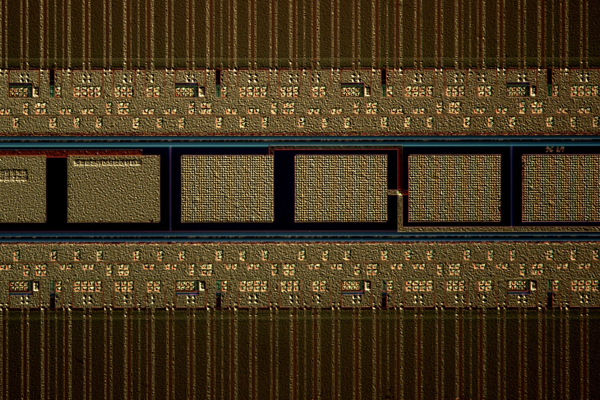
An example of how height differences on a sample surface are enhanced with DIC compared to brightfield and darkfield illumination is shown below in figure 1. DIC was used to image a patterned wafer sample. The height difference between features is more visible with DIC.

Challenges when using DIC
DIC enables users to visualize small height differences between structures on a wafer, but, for many users, it can be complex to use. The proper adjustment of the DIC prism is essential for achieving optimal contrast and accurate, reproducible results. For example, the vertical orientation of sample structures (into or out of the sample horizontal plane) in a DIC image depends greatly on the shearing of the light waves by the prism.
Therefore, the shearing influences any height difference observed between structures, i.e., whether one in the image appears to be higher or lower than another. The shearing is usually indicated as having a positive or negative bias (refer to figure 2 below), but the bias usually does not correlate with the actual height difference. For most optical microscopes, in addition to the crossing of the polarizer and analyzer, a manual adjustment of the DIC prism is required. However, users should have a high level of experience to obtain comparable, consistent DIC results. Obtaining images with very good DIC contrast can require users to spend a significant amount of time and effort doing manual adjustments.

to rise out of the surface with negative bias and recess into the surface with positive bias.
Advantages of automated and reproducible DIC imaging
For manual DIC operation, the adjustment of the microscope illumination and contrast settings must always be done directly by the users. The image results depend greatly on the level of experience and skill of the users. However, efficient wafer-inspection workflows for QC, failure analysis, and R&D can be achieved with a microscope offering automated DIC operation. Even less experienced users can easily perform reproducible DIC imaging with a minimal change of settings. At the push of a button, the appropriate prism is chosen and its position adjusted for the desired shearing of the incident light wave, plus the settings are automatically stored and then easily recalled. This feature is also essential for reliable documentation when DIC is used.
Leica solution with reproducible DIC
Quick and reliable inspection of 6-inch wafers can be achieved using a DM6 M microscope (refer to figure 3). It provides automated and reproducible DIC of wafers and semiconductor components thanks to:
- A stage specifically designed for 6-inch wafers
- An optimally crossed polarizer and analyzer (known as an ICR cube)
- Recall of exact DIC settings with motorized and encoded positioning of the prism
- Homogeneous contrast due to a dedicated DIC prism and ICR cube
- Fast and easy use as the correct prism and ICR cube is automatically selected and adjusted thanks to an automated microscope operation.
There is an additional benefit in terms of saving space in the work area, as the DM6 M has a smaller footprint than typical microscopes used for wafer inspection.

Patterned wafer images taken with a DM6 M using reproducible DIC are shown in figure 4 below. For reasons of comparison, images of the same wafer recorded with brightfield and darkfield illumination are also shown in figure 5.
 and positive (B and D) bias.")
 brightfield and B) darkfield illumination.")
A 6-inch wafer inspection microscope with automated and reproducible differential interference contrast (DIC), the DM6 M with wafer stage, was described. Wafer inspection for QC, failure analysis, and R&D in the semiconductor industry often requires optical microscopy with the use of various contrast methods. DIC enables an efficient visualization of small height differences between structures on patterned wafers. Using an automated and reproducible DIC even users with little experience can efficiently perform DIC imaging during inspection.

 and oblique (right) brightfield illumination using a Leica compound microscope. The defect on the wafer surface is clearly more visible with oblique illumination.")