Contact Us
Cross-section analysis for electronics

Cross-Section Analysis for Electronics

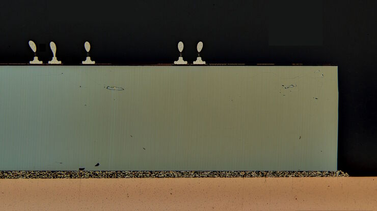
Cross-section analysis for electronics is used to examine the internal microstructure of electronic components like printed circuit boards (PCBs), assemblies (PCBAs), and integrated circuits (ICs). These components are often made from opaque, non-transparent materials. For cross-section analysis, a cross section of the component is made and analyzed with optical and electron microscopy and spectroscopy to reveal the structure and composition of grains, phases, layers, interfaces, cracks, voids, defects, etc. Cross-section analysis is useful for quality control (QC), failure analysis (FA), and research and development (R&D) of PCBs, PCBAs, ICs, and other electronic components.

Need assistance?

Contact a local imaging specialist for expert advice on cross-section analysis for your needs and budget.

Cross-section analysis is useful for quality control (QC), failure analysis (FA), and research and development (R&D) of PCBs, PCBAs, ICs, and other electronic components.

What is a cross section in manufacturing?

For cross sectioning of materials like metal alloys, ceramics, printed circuit boards (PCBs) or assemblies (PCBAs), or integrated circuits (ICs), a slice is made across its volume in a specific orientation to expose the bulk. The internal microstructure can then be observed. For PCBs and ICs, cross sectioning is useful for quality control and failure analysis.

What is a cross section of a material or product?

A cross section is a slice of a material or product, e.g., a metal, ceramic, polymer, composite material, mineral, circuit board, or integrated circuit, which allows the internal structure to be examined. A sample of the material or product is cut along a specific axis of orientation, ground, and then polished to create a smooth, flat surface. Analysis is often done with optical or electron microscopy or spectroscopy.

What is the purpose of cross sectioning?

Cross sectioning is very useful for quality control and failure analysis. It is used to evaluate the structural integrity of electronic components, like printed circuit boards (PCBs) and assemblies (PCBAs), integrated circuits (ICs), substrate materials and layers, interconnections, wire bonds, solder joints, and encapsulation materials. Cross-section analysis helps identify defects which can cause component failure.

Get your individual solution based on 3 short questions.

Dedicated configurations are available for your specific needs. Answer the short questionnaire to find the right solution for your needs. If you would rather have a representative contact you, then please click here to fill out your contact information.

Contact us

{{ question.questionText }}

Please select an answer!

Best Match

{{ resultProduct.header }}

{{ resultProduct.subheader }}

{{ resultProduct.description }}

{{ resultProduct.features }}

Request Your Information Package

Contact us

By clicking SUBMIT, I agree to Leica Microsystems GmbH's Terms of Use and Privacy Policy. I understand my privacy choices regarding my personal data as detailed in the Privacy Policy.

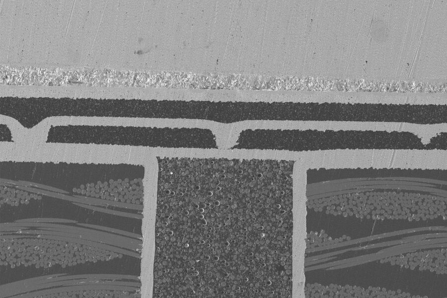
Preparation of PCB/PCBA cross section

The preparation of a PCB/PCBA cross section involves multiple steps:

  • Cutting out a slice of the printed circuit board (PCB) or assembly (PCBA) from a selected area.
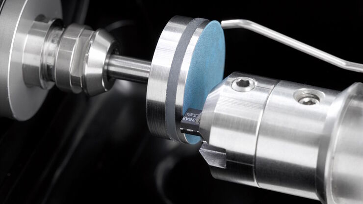
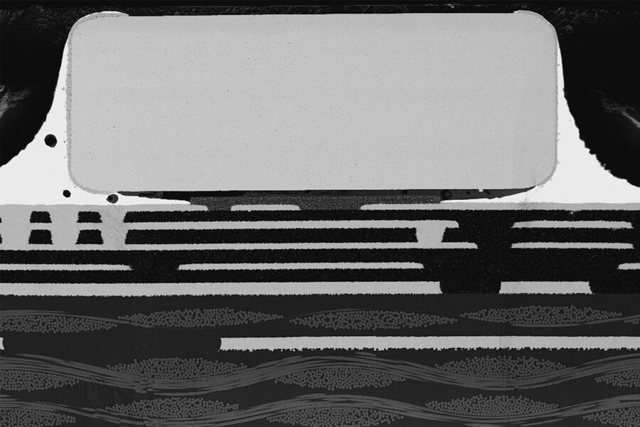
  • Cleaning, mounting, grinding, polishing, ion milling, and sometimes etching the cross section to reveal the internal microstructure and different layers of the PCB/PCBA.

The result is a smooth and flat surface that can be observed easily with optical (OM) or electron microscopy (EM). Examination with OM or EM enables assessment of the microstructure and various layers.
Preparation of IC cross section

Preparing a cross section of an integrated circuit (IC) can typically require:

  1. Selecting and cutting out a specific area to be analyzed
  2. Removal of the encapsulation materials
  3. Embedding the IC sample in an epoxy resin
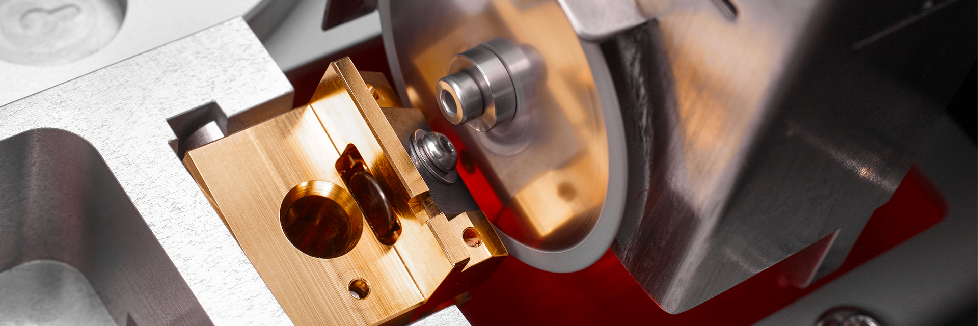
  4. Cutting out a thin slice with sawing or ion beam milling to expose the IC internal structure
  5. Grinding and polishing to obtain a smooth surface
  6. Selective etching may be used to reveal specific IC structures
  7. Visualizing and analyzing the IC cross section with optical and electron microscopy and spectroscopy, e.g., compound microscope with LIBS or SEM with EDS, to reveal the fine details and internal microstructure.

Related Articles Cross-Section Analysis for Electronics

Read our latest articles about Cross-Section Analysis for Electronics

The knowledge portal of Leica Microsystems offers scientific research and teaching material on the subjects of microscopy. The content is designed to support beginners, experienced practitioners and scientists alike in their everyday work and experiments.

More Articles
Region of a patterned wafer inspected using optical microscopy and automated and reproducible DIC (differential interference contrast). With DIC users are able to visualize small height differences on the wafer surface more easily.

6-Inch Wafer Inspection Microscope for Reliably Observing Small Height Differences

A 6-inch wafer inspection microscope with automated and reproducible DIC (differential interference contrast) imaging, no matter the skill level of users, is described in this article. Manufacturing…
Optical microscope image, which is a composition of both brightfield and fluorescence illumination, showing organic contamination on a wafer surface. The inset images in the upper left corner show the brightfield image (above) and fluorescence image (below with dark background).

Visualizing Photoresist Residue and Organic Contamination on Wafers

As the scale of integrated circuits (ICs) on semiconductors passes below 10 nm, efficient detection of organic contamination, like photoresist residue, and defects during wafer inspection is becoming…
Image of burrs (red arrows) at the edge of a battery electrode acquired with a DVM6 digital microscope.

Burr Detection During Battery Manufacturing

See how optical microscopy can be used for burr detection on battery electrodes and determination of damage potential to achieve rapid and reliable quality control during battery manufacturing.
Particles observed on the surface of a particle trap which could be used for technical cleanliness during battery production.

Battery Particle Detection During the Production Process

How battery particle detection and analysis is enhanced with optical microscopy and laser spectroscopy for rapid, reliable, and cost-effective QC during battery production is explained in this…
Particulate contamination in between moving metal plates.

Key Factors for Efficient Cleanliness Analysis

An overview of the key factors necessary for technical cleanliness and efficient cleanliness analysis concerning automotive and electronics manufacturing and production is provided in this article.
Images of the same area of a processed wafer taken with standard (left) and oblique (right) brightfield illumination using a Leica compound microscope. The defect on the wafer surface is clearly more visible with oblique illumination.

Rapid Semiconductor Inspection with Microscope Contrast Methods

Semiconductor inspection during the production of patterned wafers and ICs (integrated circuits) is important for identifying and minimizing defects. To increase the efficiency of quality control in…
Preparation of an IC-chip cross section: grinding and polishing of the chip cross section.

Cross-section Analysis for Electronics Manufacturing

This article describes cross-section analysis for electronics concerning quality control and failure analysis of printed circuit boards (PCBs) and assemblies (PCBAs), integrated circuits (ICs), etc.
Image of an integrated-circuit (IC) chip cross section acquired at higher magnification showing a region of interest.

Structural and Chemical Analysis of IC-Chip Cross Sections

This article shows how electronic IC-chip cross sections can be efficiently and reliably prepared and then analyzed, both visually and chemically at the microscale, with the EM TXP and DM6 M LIBS…
EBSD grain size distribution of the cross section of a gold wire within a silicon matrix from inside a CPU (central processing unit of a computer). The grains are highlighted with arbitrary colors.

High-Quality EBSD Sample Preparation

This article describes a method for EBSD sample preparation of challenging materials. The high-quality samples required for electron backscatter diffraction are prepared with broad ion-beam milling.
Stereo microscopes are often considered the workhorses of laboratories and production sites.

Key Factors to Consider When Selecting a Stereo Microscope

This article explains key factors that help users determine which stereo microscope solution can best meet their needs, depending on the application.

Material Analysis Microscopes

Materials analysis requires microscope solutions for the imaging, measurement, and analysis of features across a variety of materials like metal alloys, semiconductors, glass and ceramics, as well as plastics and polymers. These material analysis microscopes are important for different industrial applications, whether in quality control, failure analysis, or research and development.

Read More

Inspection Microscopes

Leica inspection microscopes cover your needs, whether it is to have an overview of a component or sample or visualize fine details.

Read More

Rating Steel Quality

Foreign substances in steel, known as non-metallic inclusions, disrupt the homogeneity of the microstructure. They can have considerable influence on the steel’s mechanical properties, affecting performance and lifetime. Therefore, rating the inclusions is important for evaluating steel quality.

Read More

Scroll to top