
Science Lab
Science Lab
The knowledge portal of Leica Microsystems offers scientific research and teaching material on the subjects of microscopy. The content is designed to support beginners, experienced practitioners and scientists alike in their everyday work and experiments. Explore interactive tutorials and application notes, discover the basics of microscopy as well as high-end technologies – become part of the Science Lab community and share your expertise!
Filter articles
Tags
Products
Loading...
. With DIC users are able to visualize small height differences on the wafer surface more easily.")
6-Inch Wafer Inspection Microscope for Reliably Observing Small Height Differences
A 6-inch wafer inspection microscope with automated and reproducible DIC (differential interference contrast) imaging, no matter the skill level of users, is described in this article. Manufacturing…
Loading...

Visualizing Photoresist Residue and Organic Contamination on Wafers
As the scale of integrated circuits (ICs) on semiconductors passes below 10 nm, efficient detection of organic contamination, like photoresist residue, and defects during wafer inspection is becoming…
Loading...
 and oblique (right) brightfield illumination using a Leica compound microscope. The defect on the wafer surface is clearly more visible with oblique illumination.")
Rapid Semiconductor Inspection with Microscope Contrast Methods
Semiconductor inspection for QC of materials like wafers can be challenging. Microscope solutions that offer several contrast methods enable fast and reliable defect detection and efficient workflows.
Loading...
 chip cross section acquired at higher magnification showing a region of interest.")
Structural and Chemical Analysis of IC-Chip Cross Sections
This article shows how electronic IC-chip cross sections can be efficiently and reliably prepared and then analyzed, both visually and chemically at the microscale, with the EM TXP and DM6 M LIBS…
Loading...
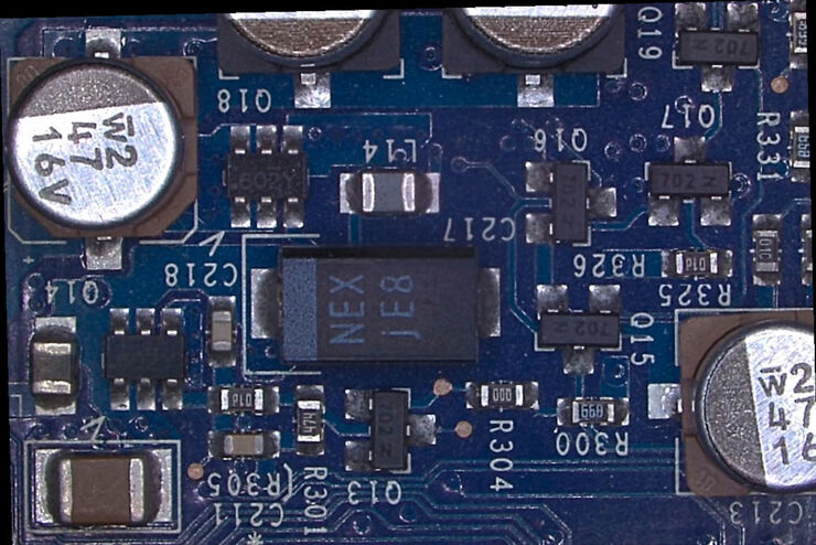
Rapid and Reliable Examination of PCBs & PCBAs with Digital Microscopy
Digital microscopes provide users with a convenient and rapid way to acquire high-quality, reliable image data and make quick inspection and analysis of printed circuit boards (PCBs) and assemblies…
Loading...

How to Boost your Microelectronic Component Inspection Performance
Do you need to see more when inspecting silicon wafers or MEMS? Would you like to get sharp and detailed sample images which are similar to those from electron microscopes?
Watch this free webinar…