Science Lab
Science Lab
Benvenuti nel portale delle conoscenze di Leica Microsystems. Troverete materiale didattico e di ricerca scientifica sul tema della microscopia. Il portale supporta i principianti, i professionisti esperti e gli scienziati nel loro lavoro quotidiano e negli esperimenti. Esplorate i tutorial interattivi e le note applicative, scoprite le basi della microscopia e le tecnologie di punta. Entrate a far parte della comunità di Science Lab e condividete la vostra esperienza.
Filter articles
Tag
Tipo di pubblicazione
Prodotti
Loading...

6-Inch Wafer Inspection Microscope for Reliably Observing Small Height Differences
A 6-inch wafer inspection microscope with automated and reproducible DIC (differential interference contrast) imaging, no matter the skill level of users, is described in this article. Manufacturing…
Loading...

Visualizing Photoresist Residue and Organic Contamination on Wafers
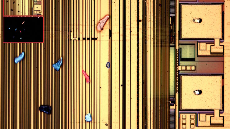
As the scale of integrated circuits (ICs) on semiconductors passes below 10 nm, efficient detection of organic contamination, like photoresist residue, and defects during wafer inspection is becoming…
Loading...

Rapid Semiconductor Inspection with Microscope Contrast Methods
Semiconductor inspection during the production of patterned wafers and ICs (integrated circuits) is important for identifying and minimizing defects. To increase the efficiency of quality control in…
Loading...

Structural and Chemical Analysis of IC-Chip Cross Sections
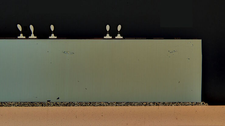
This article shows how electronic IC-chip cross sections can be efficiently and reliably prepared and then analyzed, both visually and chemically at the microscale, with the EM TXP and DM6 M LIBS…
Loading...

Rapid and Reliable Examination of PCBs & PCBAs with Digital Microscopy
Digital microscopes provide users with a convenient and rapid way to acquire high-quality, reliable image data and make quick inspection and analysis of printed circuit boards (PCBs) and assemblies…
Loading...

How to Boost your Microelectronic Component Inspection Performance
Do you need to see more when inspecting silicon wafers or MEMS? Would you like to get sharp and detailed sample images which are similar to those from electron microscopes?
Watch this free webinar…
