
Science Lab
Science Lab
Willkommen auf dem Wissensportal von Leica Microsystems. Hier finden Sie wissenschaftliches Forschungs- und Lehrmaterial rund um das Thema Mikroskopie. Das Portal unterstützt Anfänger, erfahrene Praktiker und Wissenschaftler gleichermaßen bei ihrer täglichen Arbeit und ihren Experimenten. Erkunden Sie interaktive Tutorials und Anwendungshinweise, entdecken Sie die Grundlagen der Mikroskopie ebenso wie High-End-Technologien. Werden Sie Teil der Science Lab Community und teilen Sie Ihr Fachwissen.
Filter articles
Tags
Berichtstyp
Produkte
Loading...
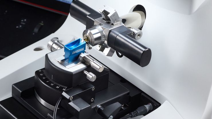
Mastering Polymer Sectioning with Helmut Gnaegi
When it comes to ultramicrotomy, few names carry the weight of Helmut Gnaegi. As co-founder of Diatome, a global leader in diamond knife technology, Helmut has spent decades refining the art and…
Loading...
Zebrafisch-Forschung
Für optimale Ergebnisse während der Bewertung, Sortierung, Manipulation und Bildgebung von Modellorganismen ist es entscheidend feine Details und Strukturen genauestens zu erkennen. Das bildet die…
Loading...
")
How to Streamline High-Plex Imaging for 3D Spatial Omics Advances
In this webinar, Dr. Julia Roberti and Dr. Luis Alvarez from Leica Microsystems introduce SpectraPlex, a new functionality integrated into the STELLARIS confocal platform for high-plex 3D spatial…
Loading...

The Guide to Augmented Reality in Microsurgery
In an era of technological advancement, Augmented Reality (AR) is rapidly transforming the medical field. In surgical microscopy, AR can display fluorescence signals as digital overlays in real-time…
Loading...

Improving Zebrafish-Embryo Screening with Fast, High-Contrast Imaging
Discover from this article how screening of transgenic zebrafish embryos is boosted with high-speed, high-contrast imaging using the DM6 B microscope, ensuring accurate targeting for developmental…
Loading...

Transforming Research with Spatial Proteomics Workflows
Spatial Proteomics, Nature Methods 2024 Method of the Year, is driving research advancements in cancer, immunology, and beyond. By combining positional data with high throughput imaging of proteins in…
Loading...
.")
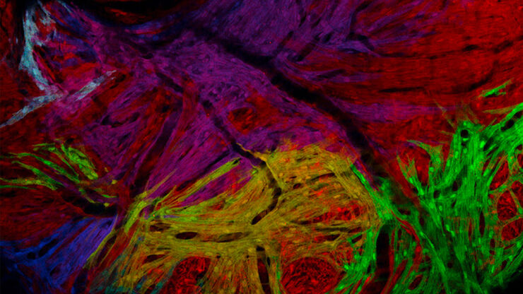
How Fluorescence Guides Sectioning of Resin-embedded EM Samples
Electron microscopes, including transmission electron microscopes (TEM) and scanning electron microscopes (SEM), are widely utilized to gain detailed structural information about biological samples or…
Loading...

Coherent Raman Scattering Microscopy Publication List
CRS (Coherent Raman Scattering) microscopy is an umbrella term for label-free methods that image biological structures by exploiting the characteristic, intrinsic vibrational contrast of their…
Loading...

Präpariermikroskope
Wenn Sie Präparationen durchführen, verbringen Sie oft viele Stunden an den Okularen eines Präpariermikroskops. Bei Leica Microsystems können Sie aus einer Vielzahl von Mikroskopen und einem…
