
Filter articles
タグ
製品
Loading...
-b-poly(isoprene). Right: Poly(styrene)-b-poly(methyl methacrylate).")
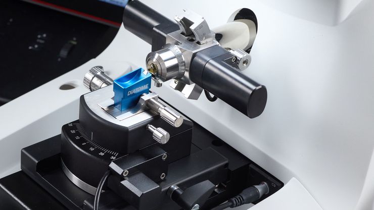
Ultramicrotome Sectioning of Polymers for TEM Analysis
We demonstrate the capabilities of the UC Enuity ultramicrotome from Leica Microsystems for preparing ultrathin sections of polymer samples under both ambient and cryogenic conditions. By presenting…
Loading...

Volume EM and AI Image Analysis
The article outlines a detailed workflow for studying biological tissues in three dimensions using volume-scanning electron microscopy (volume-SEM) combined with AI-assisted image analysis. The focus…
Loading...

Integrated Serial Sectioning and Cryo-EM Workflows for 3D Biological Imaging
This on-demand webinar explores how integrated tools can support electron microscopy workflows from sample preparation to image analysis. Experts Andreia Pinto, Adrian Boey, and Hoyin Lai present the…
Loading...

Revealing Sodium Battery Degradation via Cryo-EM and CryoFIB
Explore how cryogenic electron microscopy and focused ion beam techniques uncover the intrinsic structure of sodium battery interfaces. This webinar presents a new degradation model based on separator…
Loading...

The “Waffle Method”: High-Pressure Freeze Complex Samples
This article describes the advantages of a special high pressure freezing method, the so-called “Waffle Method”. Learn how the “Waffle Method” uses EM grids as spacers for high-pressure freezing,…
Loading...
Mastering Polymer Sectioning with Helmut Gnaegi
When it comes to ultramicrotomy, few names carry the weight of Helmut Gnaegi. As co-founder of Diatome, a global leader in diamond knife technology, Helmut has spent decades refining the art and…
Loading...
.")
How Fluorescence Guides Sectioning of Resin-embedded EM Samples
Electron microscopes, including transmission electron microscopes (TEM) and scanning electron microscopes (SEM), are widely utilized to gain detailed structural information about biological samples or…
Loading...

How to Save Time and Samples by Automated Ultramicrotomy
This article describes how 3D micro-CT data of a resin-embedded electron microscopy sample can be used to trim the specimen down to a defined target plane prior to sectioning. The interactive and…
Loading...
 and oblique (right) brightfield illumination using a Leica compound microscope. The defect on the wafer surface is clearly more visible with oblique illumination.")
Rapid Semiconductor Inspection with Microscope Contrast Methods
Semiconductor inspection during the production of patterned wafers and ICs (integrated circuits) is important for identifying and minimizing defects. To increase the efficiency of quality control in…
