

Filter articles
タグ
製品
Loading...
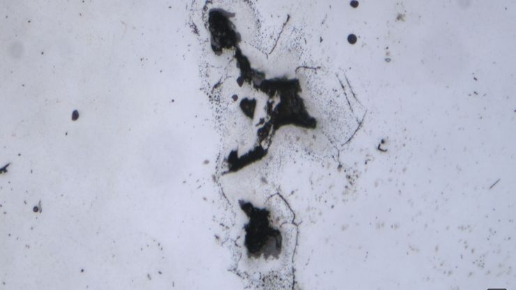
AI-Based Particle Counting with the Aivaro AI Feature Detection Software Module
The Aivaro AI Feature Detection software module enables fast manual microscope inspection of particulate contamination on various material samples. By training different classes, reflective particles,…
Loading...
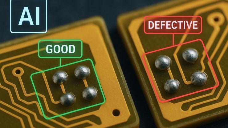
AI Image Analysis for Reliable Defect Detection
AI-based visual inspection with microscopy helps make quality control in industrial environments efficient by reducing manual inspection effort concerning defect detection, classification, and…
Loading...

An Overview of Artificial Intelligence (AI) and Machine Learning
AI is rapidly changing industrial inspection, quality control, and manufacturing workflows. But not all AI technologies work the same way. From machine learning and deep learning to the newer concept…
Loading...

Why the Future of Microscopic Inspection Is AI-Assisted, Not Fully Automated
The next wave of QC productivity gains will not come from building more automated inspection lines. Instead, it will come from augmenting millions of inspection decisions that are made manually every…
Loading...
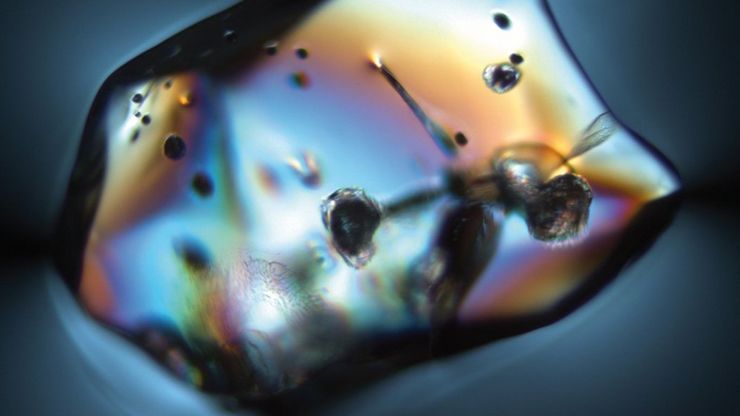
Ensuring Glass Quality with the Polarization Microscopy Advantage
Glass is one of the oldest materials known. Today, it is used for many applications, e.g., optical instruments, windows, doors, solar panels, containers for food, beverages, and medicine, so strict…
Loading...

How to Select the Right Measurement Microscope
With a measurement microscope, users can measure the size and dimensions of sample features in both 2D and 3D, something crucial for inspection, QC, failure analysis, and R&D. However, choosing the…
Loading...
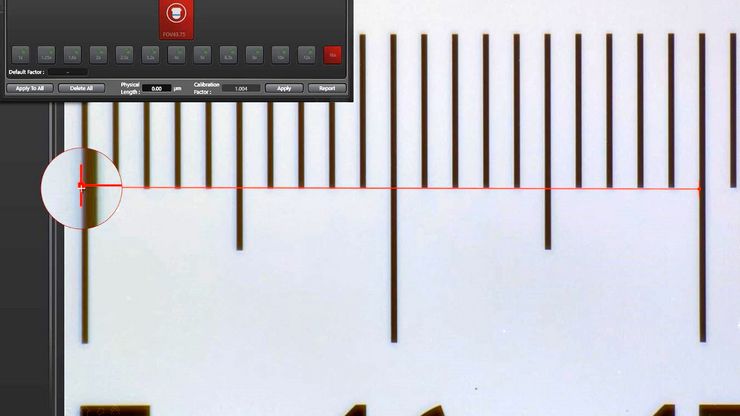
Microscope Calibration for Measurements: Why and How You Should Do It
Microscope calibration ensures accurate and consistent measurements for inspection, quality control (QC), failure analysis, and research and development (R&D). Calibration steps are described in this…
Loading...
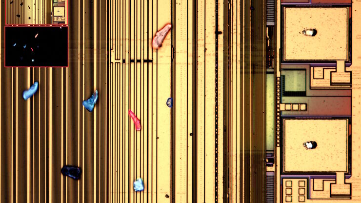
Visualizing Photoresist Residue and Organic Contamination on Wafers
As the scale of integrated circuits (ICs) on semiconductors passes below 10 nm, efficient detection of organic contamination, like photoresist residue, and defects during wafer inspection is becoming…
Loading...
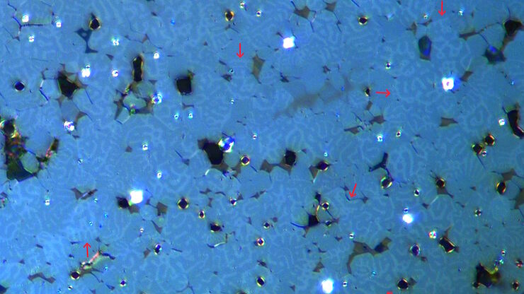
Rapidly Visualizing Magnetic Domains in Steel with Kerr Microscopy
The rotation of polarized light after interaction with magnetic domains in a material, known as the Kerr effect, enables the investigation of magnetized samples with Kerr microscopy. It allows rapid…


